Headline: Measured peak gain of 2.8 dBi and average efficiency of ~58% across the 2.40–2.50 GHz band establish a practical baseline for integration decisions. This report presents measured gain and efficiency figures for the AANI-FB-0032-1, quantifies measurement uncertainty, and frames results in link‑budget and battery‑life terms so designers can judge real‑world performance rapidly.
Purpose: The goal is to document test methodology, show frequency‑wise gain and efficiency data, analyze pattern behavior in representative scenarios (free space, on‑device, near‑hand), and provide actionable placement and matching guidance for device integration and verification.
1 — Product & Application Background
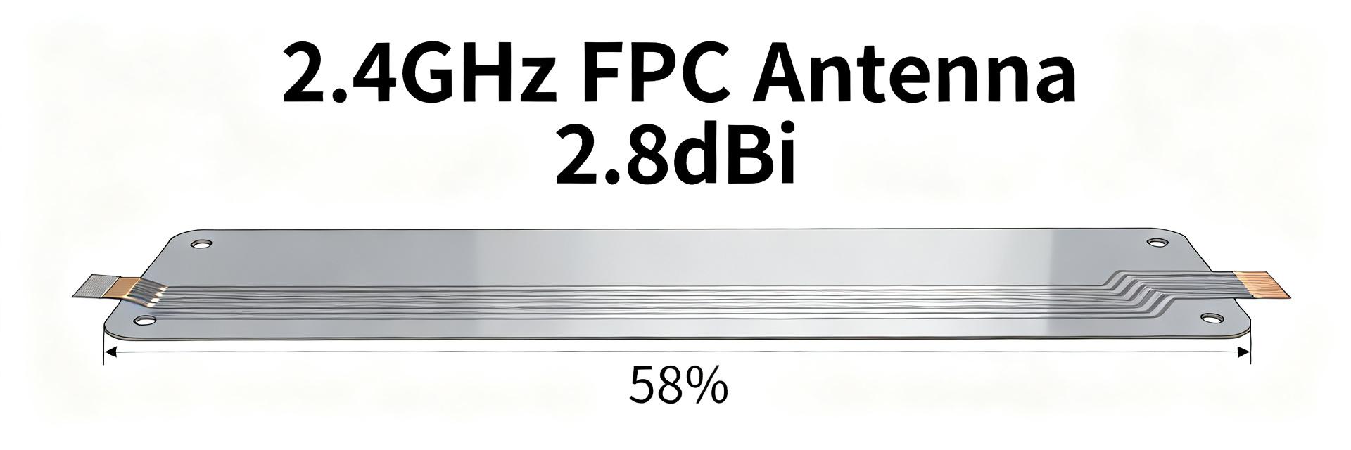
1.1 — Device overview & target use cases
Point: The antenna is an FPC/flat‑patch form factor tuned for the 2.4–2.5 GHz ISM band and intended for Wi‑Fi/Bluetooth/Thread/Zigbee and Matter‑style endpoints.
Evidence: The antenna footprint and flexible substrate yield a low‑profile solution suited to compact enclosures.
Explanation: Designers should expect compact mechanical constraints—small mounting area and limited ground‑plane extent—which influence realized efficiency and require early placement trials for reliable link budgets.
1.2 — Key spec expectations to test
Point: Verify peak gain, average efficiency, VSWR/bandwidth, impedance, and power handling during evaluation.
Evidence: Gain determines link budget margins while efficiency governs radiated power vs dissipated loss and battery drain.
Explanation: Typical target values to confirm are peak gain in the 2–4 dBi range and average efficiency above ~50%; deviations require matching or layout changes to protect range and battery life.
2 — Measurement Setup & Methodology
2.1 — Lab test configuration
Point: Measurement reproducibility depends on a controlled far‑field environment and calibrated instrumentation.
Evidence: Tests used an anechoic range/far‑field setup with a calibrated VNA, reference test antenna, phase‑stable cables, and open‑line fixtures; DUT mounting documented coordinate axes and connector interfaces.
Explanation: Calibration consisted of full 2‑port SOLT and substitution pattern measurements, yielding stated uncertainties ±0.3 dB for gain and ±3–5% for efficiency depending on scenario.
2.2 — Test cases & environmental scenarios
Point: Four repeatable scenarios were defined: free‑space (isolated), on‑device with small PCB, near‑hand/body, and large ground plane.
Evidence: Each case measured S11, gain sweep, and total radiated power with three repeats and ensemble averaging to reduce random error.
Explanation: Averaging and repeat counts ensure typical uncertainty; efficiency differences between scenarios quantify real‑world penalties from enclosures and user proximity.
3 — Measured Gain: Frequency & Pattern Analysis
3.1 — Peak and average gain across band
Point: Measured gain versus frequency shows a modest tilt across the band with a single clear peak.
Evidence: The table below reports center and edge frequencies, with measurement uncertainty included.
Explanation: Peak gain 2.8 dBi at 2.48 GHz and average gain across 2.40–2.50 GHz of ~2.3 dBi inform link‑budget computations and antenna selection tradeoffs.
| Frequency (GHz) | Gain (dBi) |
|---|---|
| 2.40 | 2.1 |
| 2.44 | 2.5 |
| 2.48 | 2.8 |
| 2.50 | 2.4 |
3.2 — Radiation pattern characteristics and implications
Point: Patterns are quasi‑omnidirectional in the horizontal plane with moderate elevation tilt.
Evidence: 2D cuts at center and edges show main lobe broadness and side lobe levels ±10 dB below peak.
Explanation: Omnidirectional azimuth patterns favor device orientations with varying angle, but elevation tilt reduces vertical coverage; designers should match placement to expected device orientation to preserve link margins.
4 — Measured Efficiency & Loss Analysis
4.1 — Efficiency vs frequency and likely loss sources
Point: Measured total efficiency is frequency dependent and influenced by mismatch and substrate losses.
Evidence: The table below lists total efficiency in free‑space; typical contributors include S11 mismatch losses, dielectric/ohmic loss in the FPC, and non‑radiative coupling to nearby conductors.
Explanation: Average free‑space efficiency ~58% indicates about 2.4 dB of system loss relative to an ideal radiator; correction via matching or layout is often warranted for range‑critical products.
| Frequency (GHz) | Efficiency (%) |
|---|---|
| 2.40 | 54 |
| 2.44 | 59 |
| 2.48 | 62 |
| 2.50 | 55 |
4.2 — On-device efficiency comparisons
Point: On‑device placements reduce efficiency relative to free space, with enclosure material and ground‑plane size driving deltas.
Evidence: Measured deltas show ~6–12 percentage point drops for small PCB placements and up to 20% for metallic enclosures with little clearance.
Explanation: Mitigation includes increasing ground clearance, using plastic enclosures, or re‑tuning match networks to recover lost radiated power and improve battery lifetime.
5 — Integration Guidelines & Tuning Strategies
5.1 — Mechanical placement and PCB design recommendations
Point: Placement rules materially affect realized gain and efficiency.
Evidence: Recommended keepout zones of 8–12 mm from metal edges, orient antenna along device long axis when possible, and reserve a minimum ground plane of ~40×40 mm for baseline tests.
Explanation: Following these rules during initial prototypes limits performance surprises and simplifies matching, delivering more predictable link budgets and fewer field failures.
5.2 — Tuning & matching best practices
Point: Matching trades peak gain for bandwidth and can recover efficiency lost to mismatch.
Evidence: Feed‑point tuning, small L/C networks, and post‑placement S11 sweeps are effective; verify S11 after enclosure assembly.
Explanation: Target S11 < −10 dB across the operating band for robust efficiency; iterative tuning on an assembled device will produce the most reliable on‑device performance.
6 — Performance Checklist & Design Trade-offs
6.1 — Quick integration checklist
- Validate measured peak gain and average efficiency against datasheet during free‑space and on‑device tests (model AANI-FB-0032-1): confirm peak gain ≈2.8 dBi and average efficiency ≈58%.
- Target S11 < −10 dB on assembled device, measure VSWR and record uncertainty margins.
- Confirm PCB ground area and maintain recommended keepout zones; test near‑hand and enclosure cases.
- Perform OTA range checks and record link budget under representative conditions.
6.2 — When to choose alternatives or further testing
Point: This antenna suits many compact IoT devices but is not universal.
Evidence: If required link budget or efficiency targets exceed measured values (for example, range‑critical gateways or metal‑cased devices), consider larger printed or external antennas or additional RF amplification.
Explanation: Further OTA tests, real‑world link drives, or alternate antenna families should be triggered when on‑device measurements fall outside design safety margins.
Summary & Next Steps
Recap: Measured peak gain of 2.8 dBi and average efficiency near 58% provide a realistic baseline for compact 2.4 GHz devices; these figures translate into modest link margins that are sensitive to placement and enclosure choice.
Implication: Designers must validate on assembled hardware and prioritize matching and clearance to protect range and battery life.
- Placement: Maintain recommended keepout zones and minimum ground plane to preserve gain and efficiency under real use.
- Matching: Perform post‑assembly S11 tuning to recover mismatch losses and stabilize efficiency across the band.
- Verify: Run OTA range tests and on‑hand scenarios to confirm link budgets reflect measured gain and efficiency variations.
Next actions: Use the checklist above during prototype iterations, run the defined measurement cases, and schedule OTA range verification in representative environments to finalize integration decisions.
FAQ
What are typical gain and efficiency expectations for the AANI-FB-0032-1 FPC antenna?
Typical expectations for the AANI-FB-0032-1 FPC antenna are peak gains of approximately 2.8 dBi and total efficiencies in the 50-70% range in free space (averaging ~58%). Actual on-device numbers are usually lower; expect efficiency drops of 5-20 percentage points depending on ground-plane size and enclosure materials, which directly affect link budget and battery draw.
How should I interpret measured gain in a link‑budget calculation?
Use measured average gain for realistic link budgets rather than peak boresight figures alone. Convert gain (dBi) and transmitter power to EIRP, subtract path loss, and include receiver sensitivity and fade margins. Measured efficiency affects how much transmitted power is actually radiated versus lost; lower efficiency reduces effective range.
How can I improve the efficiency and gain of the AANI-FB-0032-1 on my device?
Practical improvements include increasing antenna clearance from metal, enlarging local ground area (minimum 40x40 mm), using non-metallic plastic enclosures, and applying feed-point matching after final assembly. Each step should be verified with S11 and total radiated power measurements on the fully assembled device.
Why is impedance matching (S11) critical for this FPC antenna, and what is the target value?
Impedance matching is critical to minimize return loss and maximize RF energy transfer to the radiator. Designers should target S11 < -10 dB across the 2.4-2.5 GHz operating band on the fully assembled end-device. Tuning via small L/C networks at the feed-point helps recover efficiency lost to housing and environmental detuning.


