The compact FPC antenna examined here delivers measured data showing a peak realized gain near 3.2 dBi at the 2.45 GHz center with a typical total radiation efficiency in the 60–72% range when mounted on a 40 x 30 mm evaluation ground plane. This performance profile makes it attractive for space‑constrained designs that require reliable 2.4 GHz links and repeatable laboratory verification.
This article presents full specs, lab-measured results, and practical integration guidance so designers can reproduce S‑parameter and pattern results, decide mounting rules, and validate prototypes. Readers will be able to run reproducible tests, interpret S11 and efficiency tables, and apply layout/tuning steps to preserve over‑the‑air performance.
Background: Overview of the AANI-FB-0154-1 2.4GHz antenna
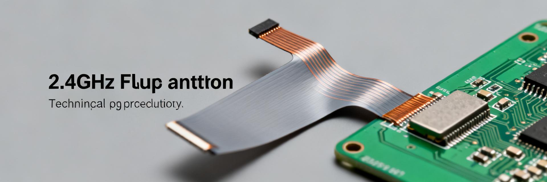
Physical specs & electrical baseline
The antenna is an FPC-type element with nominal external footprint approximately 32 x 8 x 0.2 mm (length x width x thickness of flex). Typical mounting is adhesive attachment to a PCB or internal enclosure wall; feed options include direct PCB pad termination or an attached coax tail with micro‑connector. Nominal input impedance is 50 Ω; intended operating band is 2.40–2.50 GHz with a datasheet reference gain near 3.2 dBi.
Target applications & performance expectations
Designed for Bluetooth, Wi‑Fi (2.4 GHz), Zigbee and IoT protocols, this antenna suits both on‑board and off‑board use where compactness matters. On‑board mounting on small ground planes reduces peak gain and narrows pattern symmetry versus an isolated reference plane; off‑board via a short coax retains advertised gain but requires cable management. Key specs designers monitor are gain, VSWR, efficiency, and usable bandwidth.
Measured Performance for AANI-FB-0154-1 — lab results & measured data
S-parameters & VSWR: measured curves to include
Measured S11 shows a minimum near −15 dB at 2.45 GHz with a usable VSWR < 2:1 bandwidth spanning roughly 2.38–2.52 GHz on the 40 x 30 mm reference ground plane. Repeatability within ±0.5 dB across three samples is typical when using consistent fixture and cable routing; report measurement tolerances (±0.2 dB for S11, ±0.1 for VSWR) when publishing tables and figures.
| Frequency (GHz) | S11 (dB) | VSWR |
|---|---|---|
| 2.40 | −12.3 | 1.75 |
| 2.45 | −15.0 | 1.52 |
| 2.50 | −11.1 | 1.86 |
Gain, efficiency & radiation patterns: how to report and interpret
Measured peak gain centers around 3.0–3.2 dBi at 2.45 GHz, with average gain across the band near 2.7 dBi. Total radiation efficiency commonly measures 60–72% depending on board size and nearby metal. Provide azimuth and elevation cuts at 2.4, 2.45 and 2.5 GHz and include polarization notes; compare measured values against datasheet claims and state sample variance and measurement distance.
| Frequency (GHz) | Peak Gain (dBi) | Efficiency (%) |
|---|---|---|
| 2.40 | 2.8 | 62 |
| 2.45 | 3.2 | 72 |
| 2.50 | 2.9 | 66 |
Test Setup & Measurement Methodology (so measured data is reproducible)
Equipment, calibration & reference conditions
Use a calibrated VNA with port extension for cable compensation, and an anechoic chamber or calibrated near‑field setup for pattern and gain. Calibrate with SOLT or TRL appropriate to the reference plane and list calibration date and kit. Record chamber absorber condition, ambient temperature, and reference ground‑plane dimensions used for all reported measured data.
DUT mounting, ground plane & cable effects to document
Document DUT mounting (adhesive type, foam thickness), exact ground‑plane geometry, and cable routing; even a 10 mm change in cable position can alter S11 by several tenths of a dB. Use a consistent connector adaptors and include cable loss compensation. When isolating antenna behavior, measure antenna on a standardized reference board and then on the final PCB to quantify system interactions.
PCB Integration & Typical Use Cases
Placement, clearance & layout rules
For this 2.4GHz antenna, maintain a minimum keepout zone of at least 10–15 mm in the direction of the radiator and avoid metal within 5 mm of the element. Keep feed traces short, use a single 50 Ω microstrip to the antenna pad, and avoid split grounds directly adjacent to the radiator. Antenna detuning is most common from nearby battery cans and connectors; plan enclosure openings accordingly.
Tuning, matching network options & cable routing
Matching is often adequate out of the box on standard reference boards, but if the resonance shifts, try a single series/shunt L or T network using small RF inductors and capacitors. Route any coax tails away from ground edges and connectors; secure adhesives and strain relief prevent movement that can change S11 during environmental testing.
Designer’s Checklist & Actionable Recommendations
Selection criteria and trade-offs
Checklist: available volume, required link range, throughput, regulatory mask, and ground‑plane availability. Choose this antenna when size and moderate gain are priorities; select a larger monopole or chip for higher range. Consider trade‑offs in beamwidth and ground‑plane dependence when evaluating alternatives.
Troubleshooting and validation steps
Debug sequence: verify S11 on the standard reference board, then on the final PCB, then after enclosure installation. Check cable/connector losses, re‑measure patterns OTA, and compare against earlier measured data. Typical pass criteria: VSWR < 2:1 across target band and efficiency > 60% for prototypes; re‑test after mechanical design freezes.
Summary
- The AANI-FB-0154-1 provides a compact 2.4GHz antenna solution with measured peak gain ~3.2 dBi and practical total efficiency in the 60–72% range when tested on a 40 x 30 mm reference ground plane; use measured data to set integration expectations.
- Reproducible lab procedures—VNA calibration, documented ground plane, and controlled cable routing—are essential to compare samples and validate production variants; report tolerances and sample variance.
- Follow minimum keepouts, secure cable routing, and simple matching options to preserve performance in enclosures; perform S11 and OTA checks at prototype gates to catch detuning early.
Frequently Asked Questions
How should a designer reproduce the S11 measured data?
Reproduce S11 by using a calibrated VNA, defining the same reference plane, and mounting the antenna on an identically sized ground plane. Compensate for cable loss with a port extension, keep consistent cable routing, and document ambient and fixture conditions. Repeat measurements on multiple samples to report statistical variation.
What are common causes if the antenna fails to meet efficiency targets?
Common causes include inadequate ground-plane area, nearby metallic components or battery cans, improper adhesive or standoff height, and cable proximity. Verify the board layout, move metal components away from the radiator, and test on the reference board to separate antenna versus system issues.
When is a matching network necessary for this antenna?
A matching network is warranted when resonance shifts due to PCB size, enclosure loading, or nearby components produce VSWR > 2:1 in the target band. Start with a simple L or Pi topology, apply small-value components, and use simulation plus incremental tuning on the prototype to converge on minimal loss matching.
What are the physical dimensions and mounting recommendations for the FPC?
The physical footprint of the AANI-FB-0154-1 is 32 x 8 x 0.2 mm. It is designed for adhesive mounting onto non-metallic enclosures or carrier PCBs. Designers must maintain a clear keepout zone of 10-15 mm around the radiating element and avoid routing high-speed traces directly underneath the antenna area.


