The MPFS250TS-FCG1152T2 stands out as a highly integrated, high-capacity SoC FPGA optimized for advanced system designs. Key performance parameters include ~254K logic elements, an 1152-pin FCG1152 BGA package, a robust operating temperature range from -40°C to +125°C (TJ), an integrated RISC‑V CPU subsystem, and ~128KB of on‑chip flash. This technical brief evaluates core capabilities, electrical profiles, and implementation strategies.
| Parameter | Headline Value |
|---|---|
| Logic Elements | ~254K |
| Package | FCG1152 (1152-pin BGA) |
| Temp Range (TJ) | -40°C to +125°C |
| Embedded CPU | RISC‑V Subsystem |
| On‑Chip Flash | ~128KB Footprint |
1 — Background & Device Overview
Package & Pinout Snapshot
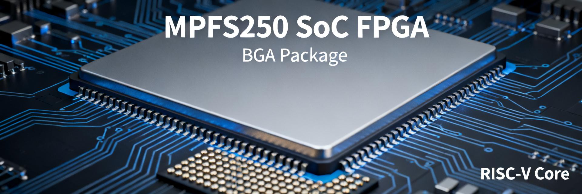
The physical and electrical layout of the FCG1152 BGA package directly influences PCB assembly and thermal management decisions. Sporting 1152 package balls alongside a central thermal pad and organized I/O banks, this configuration demands highly controlled land patterns and thermal via designs. Engineers must carefully allocate power rails to individual banks, dedicate internal PCB plane layers for clean return paths, and establish clear BGA assembly constraints early in the stackup phase.
Core Architecture Summary
The hardware architecture partitions the FPGA fabric, CPU subsystem, memory, and high-speed transceivers to balance real-time compute requirements against external I/O throughput. Armed with ~254K logic elements, integrated multi-core RISC‑V processors, distributed SRAM blocks, dedicated DSP slices, and high-speed SERDES lanes, the platform is designed for heterogeneous workloads. The programmable fabric handles parallel datapath acceleration while the CPU manages overall system control.
2 — Electrical & Thermal Performance
Power Consumption: Static vs. Dynamic
Operating power varies substantially based on logical states, clock rates, and active interfaces. Static power is stable and typically registers in the single-digit watt range at idle. Dynamic power, however, scales quickly with fabric utilization, operational frequency, and transceiver utilization. Designers should establish clear profiles across different operational phases, tracking both die-level behavior and overall system board-level consumption.
Thermal Behavior & Operating Envelope
An extended junction temperature limit of up to +125°C demands a rigorous thermal mitigation strategy. Continuous processing under high workloads causes rapid junction temperature rises, which can trigger thermal-related performance degradation. System developers must integrate thermal vias, large dedicated board copper planes, active heatsinks, or forced convection cooling to handle continuous operational loads while leaving safety margins for transient burst processing.
3 — FPGA Fabric & Compute Performance
Logic, DSP & Timing Characteristics
Overall throughput relies on optimal configuration of the integrated fabric blocks. The ~254K logic elements yield high logic gate equivalents that seamlessly interface with the DSP array. Achieving target clock frequencies of hundreds of MHz requires careful logic design, pipelining, and routing constraint management. Designers should focus on balancing registers, isolating high-fanout nets, and timing path optimization.
Benchmarks & Test Methodology
Evaluating hardware configurations demands reproducible, workload-based test suites. The benchmarks must utilize fixed synthesis configurations, representative bitstreams (such as multi-stage DSP pipelines, parallel packet parsers, or accelerator kernels), and structured memory access patterns to isolate and measure true hardware efficiency.
| Workload | Utilization | Clock Speed | Throughput | Power |
|---|---|---|---|---|
| DSP Pipeline | 45% | 300 MHz | 12 Gops | 6.5 W |
| Packet Parser | 30% | 250 MHz | 20 Gbps | 5.0 W |
4 — I/O, Transceivers & Memory Interfaces
High-Speed Transceivers & I/O Capabilities
The multi-lane SERDES transceivers provide multi-gigabit throughput paths to external systems, making layout-level signal integrity (SI) design essential. High-speed signals require tight impedance control, matched routing lengths, and minimal layer transitions. System designers should run post-layout simulations, evaluate optical eye diagrams, and run Bit Error Rate Testing (BERT) to prove interface stability.
External Memory & Peripheral Interfaces
External dynamic memories require precise clock-to-data calibration. Layouts must accommodate timing tolerances, trace routing rules, and impedance match networks for DDR interfaces. In addition, secondary non-volatile storage, like QSPI or parallel flash, must be verified to ensure boot stability and reliable runtime loading.
5 — Real-World Application Case Studies
Industrial & Aerospace (Thermal-Stressed Compute)
In harsh industrial or aerospace settings, system stability is prioritized above all else. Under continuous processing loads (using transceivers and memory controllers simultaneously), typical board power ranges from 8W to 12W. Key design practices include strict hardware rail sequencing, thermal via grids placed under the BGA, and careful clock derating to ensure safety margin across the entire operating range.
Edge Networking / Packet-Processing Example
For high-speed edge networking, pairing custom DMA controllers with dedicated packet parsing engines leverages the transceiver lanes to handle double-digit gigabit streams. Achieving sub-microsecond latency requires optimizing DMA transaction lengths, aligning internal FIFO depths, and efficiently partitioning software interrupts across the RISC-V CPU subsystem.
6 — Design Recommendations & Post-Silicon Checklist
PCB, Power Delivery & Mechanical Checklist
- Allocate dedicated power planes for Core, PLL, and Transceiver power rails.
- Place low-ESR decoupling capacitors directly beneath the FCG1152 BGA pins.
- Incorporate high-density thermal via arrays under the device thermal pad.
- Set physical component keepouts around the BGA to accommodate optional heatsinks.
Performance Tuning & Verification Checklist
- Analyze post-route timing reports for critical paths and routing bottlenecks.
- Enable and tune active DDR controller calibration routines.
- Run extensive BERT tests and capture transceiver eye diagrams under hot/cold cycles.
- Track dynamic current draw on main power lines during simulated worst-case operations.
Summary
The MPFS250TS-FCG1152T2 delivers an exceptional balance of logical fabric density, a low-power RISC‑V CPU subsystem, and high-speed serial connectivity in a package built for industrial temperatures. To fully exploit these capabilities, designs require careful PCB layouts, systematic thermal-structural analysis, and methodical interface validation. Implement the recommended checklists, and monitor real-world power profiles during bring-up to ensure long-term, high-efficiency deployment.
Frequently Asked Questions
What are the core specifications of the MPFS250TS-FCG1152T2?
The MPFS250TS-FCG1152T2 is a high-capacity PolarFire SoC FPGA featuring ~254K logic elements, a multi-core RISC-V CPU subsystem, ~128KB of on-chip flash, and is packaged in an 1152-pin FCG1152 BGA package with an extended operating temperature range (TJ) of -40°C to +125°C.
What are the MPFS250TS-FCG1152T2 power consumption characteristics?
Expect wide variance between states. Idle power is in the low single-digit watts, mid-load fabric activity typically adds several watts, and heavy multi-lane transceiver or DDR interface usage can drive board-level power consumption into double-digit wattages (typically 8-12W).
How should designers validate MPFS250TS-FCG1152T2 thermal performance?
Thermal validation must combine junction-to-board simulation with physical testing. Implement extensive thermal via arrays, large copper pours, and active heatsinking or forced-air cooling, then measure actual temperatures via junction sensors and thermal cameras under real-world workloads.
What benchmarking approach is recommended for performance evaluation?
Run repeatable, workload-based benchmarks including DSP pipelines, packet parsers, and memory-intensive accelerators under fixed toolchain parameters. Measure and report resource utilization, clock frequency, actual throughput, and end-to-end power consumption to establish design trade-offs.


