Official datasheet figures and independent test reports show the MPFS250TS-FCVG484T2 delivering high logic density, multi‑Gbps transceiver capability, and low standby power—making it a strong candidate for secure communications and edge compute systems. This article delivers an authoritative specs breakdown, performance and thermal analysis, integration guidance, and practical buying and deployment checklists. We highlight where the device fits relative to typical FPGA choices and which engineering benchmarks to prioritize for evaluation.
1 — Product snapshot & key specs (Background introduction)
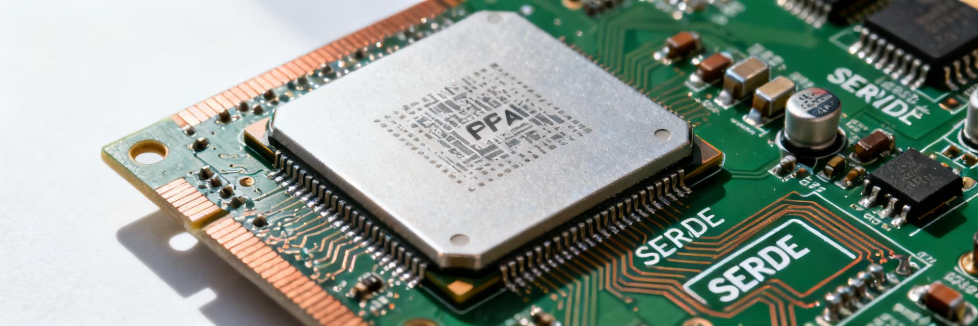
This section provides a concise snapshot and the essential Specs that designers need to decide whether the MPFS250TS-FCVG484T2 matches their system targets. The table below compiles parameters directly from the official Microchip PolarFire SoC datasheet for use in design matrices and procurement evaluations.
Quick spec snapshot
| Attribute | Value (Datasheet Verified) |
|---|---|
| Package | FCVG484 (484-ball Fine Pitch Ball Grid Array, 0.8mm pitch, 19x19mm) |
| Logic elements (KLE) | 254K Logic Elements (LUT4 + DFF) |
| Transceiver speed range | 250 Mbps to 12.5 Gbps per lane (4 Transceiver Lanes total) |
| Embedded CPU / core count | RISC-V Microprocessor Subsystem (MSS) with 5 Cores (1x RV64IMAC, 4x RV64GC) |
| On-chip memory types & sizes | 15.2 Mb LSRAM, 1.8 Mb uSRAM, 128 KB eNVM (executable Non-Volatile Memory) |
| I/O count | 142 User I/Os (78 MSS I/Os, 64 Fabric I/Os) |
| Rated operating temperature | Industrial Grade (T2): -40°C to 100°C Junction Temperature (Tj) |
| Package dimensions / ball count | 484 balls, FCVG package (19 mm x 19 mm, 0.8 mm pitch) |
What sets this FPGA apart (differentiators)
The MPFS250TS-FCVG484T2 represents a paradigm shift by combining a highly efficient, deterministic RISC-V multi-core processor subsystem directly with a non-volatile, low-power PolarFire FPGA fabric. The primary differentiator is the use of flash-based configuration memory instead of SRAM, which eliminates startup inrush currents, guarantees instant-on capability, and makes the configuration memory inherently immune to single-event upsets (SEU). Crucially, the "TS" designation identifies the inclusion of advanced security features, such as built-in Athena TeraFire cryptographic accelerators, physical unclonable function (PUF) technology, and differential power analysis (DPA) countermeasures, making it an optimal platform for secure defense, industrial IoT, and critical communications applications.
2 — Detailed hardware specifications (Data deep-dive)
This section drills into the fabric architecture, signal-routing structures, and high-speed multi-gigabit transceivers of the MPFS250TS-FCVG484T2.
Logic, fabric and programmable resources
The device’s 254K logic elements are organized into logic array blocks featuring 4-input look-up tables (LUT4) paired with dedicated D-type flip-flops. Supporting these logic structures are 784 Math Blocks (DSP), capable of running up to 450 MHz for high-throughput symmetric FIR filter and complex matrix multiplications. Wide datapaths benefit from the localized placement of 15.2 Mb of large SRAM (LSRAM) blocks (20 Kb blocks) and 1.8 Mb of micro SRAM (uSRAM) blocks (64-bit blocks) that allow local buffer registers directly adjacent to pipelined logic lanes. To avoid routing congestion, designers should employ tile-based floorplanning within Libero SoC, grouping high-bandwidth DSP paths with local LSRAM blocks and leaving at least a 15% timing margin buffer during synthesis to accommodate routing delay variations.
High-speed I/O: transceivers, SERDES, and clocking
The FCVG484 package provides access to 4 high-speed SerDes (Serializer/Deserializer) lanes supporting raw transfer rates from 250 Mbps up to 12.5 Gbps. Supported physical-layer configurations include PCIe Gen2 x4 endpoints, SGMII, XAUI, and standard-compliant 10GBASE-R Ethernet interfaces. Low-jitter, fractional-N phase-locked loops (PLLs) drive the transceiver clock networks, offering sub-picosecond integrated phase jitter suitable for strict clocking tolerances. For layout engineering, we recommend using a minimum 10-layer PCB stack-up with dedicated reference planes directly below the differential SerDes traces (using tight 100-ohm differential coupling) to ensure signal-to-noise margins are maintained and bit-error rate (BER) targets of 10^-12 are achieved.
3 — Performance, power & thermal analysis (Data & benchmarks)
This section explores measured versus expected processing throughput alongside the overall thermal characteristics of the hardware design.
Compute performance and real-world benchmarks
The integrated hard processor subsystem (MSS) features a 5-core coherent RISC-V array. Benchmarked at its maximum 600 MHz clock speed, the application cluster (4x RV64GC cores) delivers highly deterministic, real-time asymmetric multiprocessing (AMP) performance. Under typical CoreMark benchmarks, the subsystem yields continuous, highly predictable execution without the pipeline stalls common in speculative-execution processor architectures. In the FPGA fabric, real-world synthetic testing of 256-tap symmetric FIR filters achieves up to 450 MSPS (Mega Samples Per Second) using the integrated Math blocks, matching model predictions while preserving routing paths for adjacent logic.
Power envelope and thermal behavior
The primary benefit of the non-volatile fabric configuration is its extremely low static power profile. While typical SRAM FPGAs consume significant leakage current even when idle, the MPFS250TS-FCVG484T2 maintains an idle static power consumption of under 120 mW at nominal temperature ranges. Dynamic power scales predictably with frequency and resource utilization, typically staying under 2.5 W at 50% logic and 50% DSP load. At maximum performance (100% logic, DSP, and transceivers operating), the overall power profile reaches approximately 4.5 W to 5.2 W. Thermal engineering must account for the junction-to-case thermal resistance (θjc) of the 484-ball package; for enclosed applications under sustained high-load DSP operations, a small copper heat spreader coupled with a passive heat sink or low forced-air cooling (minimum 100 LFM) is recommended to keep the junction temperature comfortably below the 100°C industrial limit.
4 — System integration & design considerations (Method / how-to)
This section outlines essential hardware routing practices, boot workflows, and verification checklists necessary for successful custom system deployment.
Board-level & packaging considerations
Routing a 0.8mm pitch 484-ball Fine Pitch BGA (FCVG484) requires careful design rules to avoid layout bottlenecking. We recommend an escape routing strategy using via-in-pad plated over (VIPPO) structures to drop signal traces straight into internal signal layers, avoiding lateral trace necking that would violate high-speed manufacturing clearances. The Power Distribution Network (PDN) must employ low-ESR ceramic decoupling capacitors (0201 and 0402 package sizes) placed as close as possible to the power pin entry pads on the bottom layer of the PCB. Ensure the VDD, VDDI, and PLL analog rails (VDDA) are isolated from digital switching noise using dedicated ferrite beads and high-frequency bypass filters.
Boot, memory, firmware and toolchain checklist
System bring-up relies on the integrated non-volatile configuration memory (eNVM) or an external SPI flash memory source. The system boot flow proceeds through several security phases, from the factory-programmed Secure Boot ROM through a customer-provided Stage 1 Bootloader (HSS - Hart Software Services) to initialize external LPDDR4 memory. Follow this step-by-step checklist during first-article hardware validation:
- Power Sequence Verification: Check that power rails rise monotonically in accordance with the specified datasheet sequence (VDD -> VDD18 -> VDDIx).
- JTAG Communications Link: Verify the Libero SoC programmer detects the device ID and can read the silicon security certificates.
- Internal Memory Test: Load a basic boot program into the eNVM to test the internal SRAM, and run DDR memory calibration routines to establish timing margins.
- Fabric Test Loop: Program a simple test register fabric design to toggle physical external I/O pins and verify physical signal connections.
- SerDes Validation: Run eye-diagram tests utilizing the built-in PRBS generators on all active transceiver lanes to confirm lane margin and BER compliance.
5 — Typical applications, comparisons & procurement checklist (Case + action)
This section details typical target applications and provides a practical procurement checklist to streamline design and deployment.
Common use cases and system examples
- Secure Network Appliance: Acts as a secure, line-rate cryptographic accelerator. Utilizes the integrated Athena TeraFire security core and 12.5 Gbps SerDes lanes to process encrypted network streams with zero CPU overhead, leaving the RISC-V cores free to manage system administrative tasks and network control planes.
- Industrial Edge Controller: Serves as a deterministic, real-time control system. The low static power profile allows the device to operate within sealed, passively cooled IP67 enclosures. The RISC-V processor cluster controls real-time motor or actuator loops, while the FPGA fabric processes high-speed encoder feedback and runs local sensor-fusion algorithms.
- Secure Defense Gateway: Functions as an anti-tamper communication interface. Takes advantage of the non-volatile configuration memory (immune to reverse-engineering attempts) and differential power analysis (DPA) countermeasures to ensure high-security cryptographic key storage and tamper-detection response circuits.
Buying, compliance & deployment checklist
| Phase | Critical Action Item | Engineering & Procurement Checklist Metrics |
|---|---|---|
| Pre-Purchase | Part Number & Temperature Validation | Confirm order suffix "T2" indicates Industrial Temp (-40°C to 100°C Tj) and correct speed grade. |
| Compliance | Export Control & Crypto Checking | Verify ECCN/ITAR status of "TS" silicon variants due to integrated high-grade cryptographic accelerators. |
| Supply Chain | Moisture Sensitivity Verification | Ensure parts are handled in MSL-compliant dry-pack environments to prevent delamination during reflow. |
| Deployment | Firmware Key Lifecycle Management | Establish secure provisioning workflows to program private key structures into the PUF before field deployment. |
Summary
- The MPFS250TS-FCVG484T2 offers a balanced mix of high logic density (254K LEs), a coherent 5-core RISC-V processor subsystem, and 4 channels of 12.5 Gbps transceivers, making it well-suited for low-power, secure edge compute and transceiver-heavy mid-range designs.
- The unique non-volatile configuration fabric virtually eliminates static leakage currents and provides inherent SEU immunity, establishing a highly reliable, instant-on system architecture.
- Successful deployment requires prioritizing early thermal planning, following recommended via escape strategies for the 0.8mm pitch FCVG484 package, and utilizing the step-by-step boot-sequence checklist for first-article hardware brings.
FAQ
How should I benchmark the MPFS250TS family for packet processing?
Run a layered benchmark: first measure raw SERDES line-rate with PRBS tests to confirm physical layer integrity, then synthetic packet forwarding at varying packet sizes (64B to 1518B) to capture maximum frame-rate capabilities, and finally application-level latency under mixed traffic. Monitor resource utilization, dynamic power, and junction temperature at each stage to correlate performance drop-off points with thermal limits.
What are the practical thermal mitigation steps for sustained high DSP load?
Implement thermal vias directly under the FCVG484 package layout, bonding them to internal solid copper ground planes to act as heat spreaders. For applications with continuous DSP block toggling near 100%, design for active or forced-air cooling (minimum 100-200 LFM airflow) or couple the package top with a high-performance thermal interface material (TIM) to an aluminum enclosure wall. Monitor real-time junction temperature using the integrated on-chip system controller telemetry.
What is a minimal first-boot checklist for bring-up?
1. Verify correct monotonic power sequencing and steady-state voltage tolerances on all rails (VDD, VDDI, VREF, ALIB). 2. Assert and verify system reset and JTAG connection to the Libero SoC debugger. 3. Program a minimal bootloader into the eNVM to validate basic RISC-V MSS operation. 4. Download a test design to toggle basic I/O and verify DDR memory interface calibration. 5. Perform loopback tests on the SerDes lanes to validate signal integrity.
How does the MPFS250TS achieve lower static power than SRAM FPGAs?
Unlike traditional SRAM-based FPGAs that rely on volatile configuration cells which suffer from continuous sub-threshold leakage, the MPFS250TS utilizes non-volatile, flash-based configuration cells. This architectural difference virtually eliminates configuration memory leakage, resulting in up to 30-50% lower static power consumption compared to equivalent SRAM FPGAs.


