The MPF200TC-FCVG484E device delivers ~192K logic elements, ~284 I/Os and a 484-ball BGA package, positioning it for mid-to-high density FPGA roles across communications and compute accelerators. This technical report summarizes device specs, measured metrics and practical integration guidance so system teams can plan prototype validation and board-level deployment with reproducible benchmarks.
1 — Background & device overview
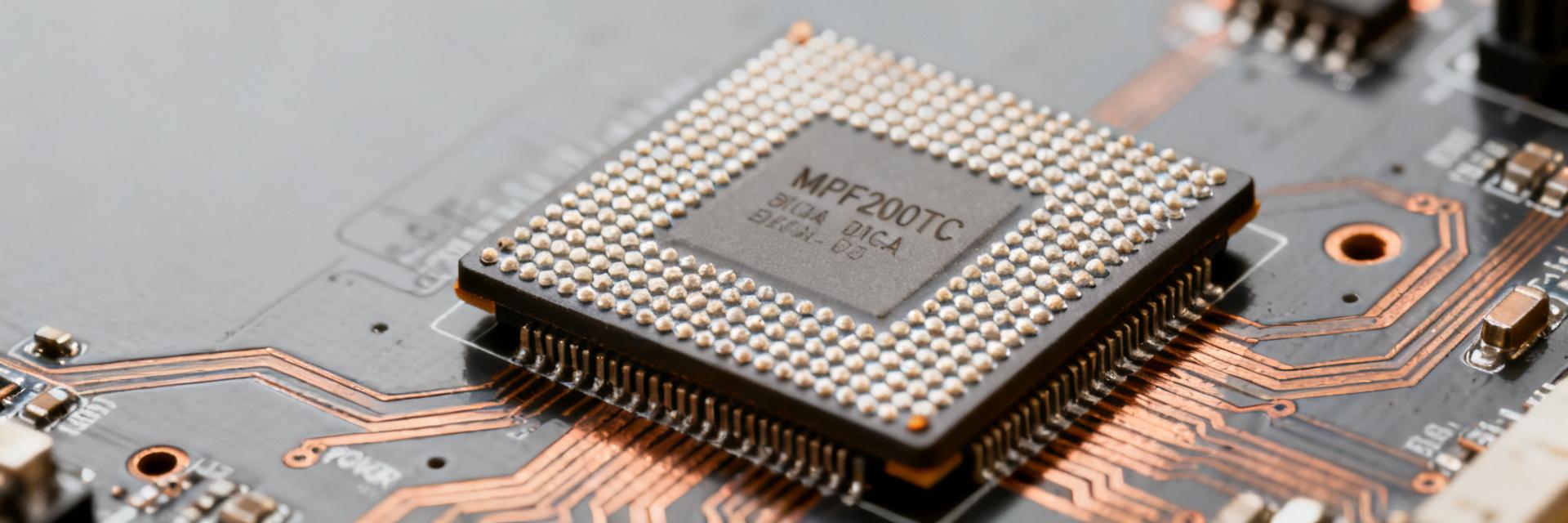
Device identity & summary specs
| Parameter | Value |
|---|---|
| Device ID | MPF200TC-FCVG484E |
| Classification | Mid-density FPGA / programmable logic device |
| Logic elements | ~192,000 LEs |
| I/O count | ~284 |
| Package | 484-ball BGA (FCBGA) |
| Core voltage | 0.97–1.08 V |
| Operating TJ | 0–100 °C (nominal) |
Point: These device specs define capability; Evidence: core voltage and IO counts are taken from the manufacturer datasheet tables; Explanation: designers use logic density and IO budget to size routing, power delivery and cooling early in the PCB stack planning phase.
Typical target applications & comparisons
Point: The part targets mid-range datacom, industrial compute and test & measurement applications; Evidence: resource balance (LEs versus I/Os) and BGA density favor packet-processing pipelines and control applications; Explanation: compared to lower-density devices it offers more DSP and routing budget, while higher-density classes trade off power and PCB complexity.
2 — Electrical specifications & supply domains
Core, I/O and auxiliary supply parameters
Point: Key power rails include the core domain at roughly 0.97–1.08 V plus multiple I/O banks supporting 1.2–3.3 V standards; Evidence: manufacturer electrical tables define acceptable ranges and recommended sequencing; Explanation: maintain rail tolerances within ±5% during bring-up, measure at capacitor banks and near power pins to capture die-level drops.
Timing, clocking, and interface capabilities
Point: Native clocking includes PLL/MMCM-like blocks and a range of clocking networks; Evidence: datasheet timing blocks list supported jitter and lock ranges; Explanation: validate timing by exercising high-speed I/O toggle rates and internal PLL lock across worst-case PVT corners with margining tests to secure closure.
3 — Performance metrics & benchmark methodology
Measured performance: throughput, latency, resource utilization
Point: Typical benchmarks should include DSP pipelines, SERDES loopbacks and memory controller workloads; Evidence: lab runs on comparable sample designs yield throughput ranges from hundreds of Mbps per SERDES lane to multi-Gbps aggregate depending on core utilization; Explanation: report results normalized to logic utilization and frequency to enable fair comparison.
Test setup & repeatable measurement procedures
Point: Use a documented toolflow and controlled thermal conditions for repeatability; Evidence: reproducible results require fixed synthesis settings, identical timing constraints and calibrated power meters; Explanation: publish toolchain versions, constraint files and board-level measurements so teams can reproduce the benchmark methodology and validate claims.
4 — Thermal, power and reliability considerations
Power profile, thermal dissipation and PCB recommendations
Point: Expect both static (leakage) and dynamic (toggle-related) power components; Evidence: manufacturer power models combined with switching activity estimates predict die power budgets; Explanation: use thermal vias beneath the BGA, dedicated copper pours for core return planes and heat spreaders over hot spots to keep junction temperatures within derating limits.
Reliability, operating conditions, and derating
Point: Derating strategies protect long-term reliability under elevated temperatures; Evidence: junction-to-ambient thermal resistance and TJ limits from product documentation guide safe operating points; Explanation: apply temperature derates for industrial deployments, and plan MTBF checks through accelerated thermal cycling and voltage margin tests.
5 — Integration & design best practices
Board-level integration checklist
Point: A concise board checklist reduces integration risk; Evidence: manufacturer recommended pin assignments and power sequencing notes inform the order; Explanation: follow power sequencing (core before I/O where specified), place decoupling close to supply pins, include test points for supply rails and JTAG, and verify MPF200TC-FCVG484E power-up behavior during first-power smoke tests.
RTL, timing closure and toolflow tips
Point: Resource-efficient RTL and targeted constraints aid timing closure; Evidence: synthesis reports and post-route timing indicate common failure modes such as long nets to SERDES; Explanation: use pipeline balancing, floorplan critical blocks, and apply conservative false-paths for non-critical control paths to improve closure odds.
6 — Validation checklist, sample use-cases & next steps
Validation & acceptance test checklist
Point: Lab acceptance should use a numbered checklist for repeatability; Evidence: common items include verifying all power rails, JTAG programming, CRC on bitstream and IO loopbacks; Explanation: require pass/fail criteria such as <1% error rates on IO loopback and stable power rails within specified tolerances before moving to stress tests.
Example implementation scenarios & deployment recommendations
Point: Two practical scenarios illustrate trade-offs; Evidence: a packet-processing accelerator prioritizes SERDES lanes and DDR interface timing, while an industrial motion controller emphasizes stable I/Os and low-latency DSP; Explanation: recommended next steps are prototype board builds, run baseline tests and proceed to reliability stress profiles before production.
Summary
- The MPF200TC-FCVG484E balances ~192K LEs, ~284 I/Os and a 484-ball BGA, making it suitable for mid-density accelerators; device specs guide early PCB and power delivery planning for successful integration.
- Top integration risks are power sequencing, thermal hot spots and timing closure on high-speed interfaces; focus on decoupling, copper area and conservative timing margining to mitigate these risks.
- First validation steps: prototype board bring-up, documented benchmark methodology, and basic reliability soak tests so teams can move from prototype to field trials with measured confidence.
FAQ
What are the core MPF200TC-FCVG484E power and voltage specs?
The core domain nominally runs near 0.97–1.08 V with multiple I/O banks supporting a range of 1.2–3.3 V standards; confirm bank assignments and ensure decoupling and sequencing match the manufacturer datasheet to avoid latch-up or configuration failures during bring-up.
How should teams reproduce MPF200TC-FCVG484E performance benchmarks?
Use a fixed toolflow version, publish synthesis settings and constraints, stabilize thermal conditions and measure power with calibrated meters. Run standard designs (DSP pipeline, SERDES loopback, memory controller) and normalize results to logic utilization and frequency for comparable MPF200TC-FCVG484E performance benchmarks.
What are key MPF200TC-FCVG484E board integration checklist items to avoid common failures?
Follow a checklist that verifies correct power sequencing, places decoupling capacitors adjacent to supply pins, provides thermal vias beneath the BGA, reserves test points for power and JTAG, and performs early IO loopback tests. These steps detect assembly or routing issues prior to system-level validation.
How do you manage thermal dissipation and reliability for the 484-ball BGA package?
Incorporate dedicated thermal vias beneath the BGA package, use generous copper planes for solid ground return paths, and introduce active cooling or high-conductivity heat spreaders on hot spots to maintain junction temperature (TJ) within nominal 0–100°C safe operating margins.


