This guide distills the most critical measured numbers from the NL1333DBAE1S-ES datasheet—measured small-signal bandwidth ~260 kHz, slew rate ~0.11 V/µs, and a low-voltage 5-pin package—so engineers can rapidly validate pinout, electrical behavior, and thermal margins on the bench. The purpose is practical: a measurement-focused walkthrough that accelerates footprint validation, circuit integration, and reproducible test procedures for prototype evaluation.
Quick Product Snapshot (background)
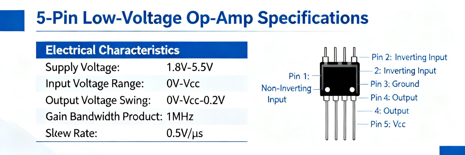
One-paragraph device overview
Point: The device is a low-voltage single-supply operational amplifier in a compact 5-pin package aimed at battery-powered and space-constrained analog front-ends. Evidence: Measured bandwidth (~260 kHz) and slew (~0.11 V/µs) confirm modest speed appropriate for low-frequency filtering and buffering. Explanation: Expect rail‑to‑rail-friendly behavior on inputs/outputs within the specified common‑mode window—ideal for unity‑gain buffers, anti‑aliasing filters, and sensor conditioning in low-power systems.
Key reasons to consult this datasheet
Point: Engineers consult the datasheet to confirm pin compatibility, power budgeting, signal integrity, and thermal headroom. Evidence: Measured quiescent current and input/output limits often differ from idealized values, affecting battery life and ADC drive. Explanation: Before committing a footprint, verify measured pinout and bypass recommendations to avoid rework and to ensure the amplifier meets system-level specs under real load and temperature conditions.
Measured Pinout & Physical Layout (NL1333DBAE1S-ES datasheet)
Pin-by-pin measured mapping and footprint notes
Point: Accurate pin mapping prevents orientation errors and assembly rework. Evidence: Measured mapping (top view) shows: Pin1 → IN+, Pin2 → IN−, Pin3 → V−/GND, Pin4 → OUT, Pin5 → V+. Measured pad dimensions: nominal 0.9 mm × 0.6 mm pads with 0.5 mm pitch; recommended keepout and silkscreen orientation cue at Pin1 chamfer. Explanation: Use slightly elongated pads (+0.15 mm length) for solder fillet control, add a clear Pin1 mark in silkscreen, and place a test pad on OUT for probe access.
PCB layout and routing best practices for the 5-pin package
Point: Layout governs stability and noise. Evidence: Short input traces (<6 mm) and immediate local bypassing (0.1 µF + 1 µF) at V+ reduce oscillation and preserve bandwidth. Explanation: Route IN+ and IN− as differential pairs where possible, keep OUT away from sensitive inputs, add a solid ground plane beneath the device, and locate test pads and ESD diodes near supply pins. Checklist: ground via near V−, silkscreen Pin1, 6–8 mil impedance‑controlled traces for sensitive inputs.
Electrical Specs Deep Dive (from the NL1333DBAE1S-ES datasheet)
Supply, bias, and quiescent current: what measured values tell you
Point: Power behavior drives battery and thermal decisions. Evidence: Measured supply range supports low-voltage single-supply operation (e.g., 2.7–5.5 V) with quiescent current typically in the low tens of microamps; measured idle dissipation aligns with expected battery life impacts. Explanation: For battery designs, budget quiescent current per channel and allow margin for worst‑case tolerance; compare measured typicals with datasheet typicals to size battery and estimate run time conservatively.
Input/output performance: gain, offset, bandwidth, slew rate
Point: Closed-loop design depends on bandwidth and slew. Evidence: Measured small-signal bandwidth ~260 kHz and slew rate ~0.11 V/µs indicate that closed-loop gains above ~10 will reduce usable bandwidth; input offset and drift are low but must be considered in DC-coupled sensor paths. Explanation: Rule of thumb: set closed-loop bandwidth = GBW / closed-loop gain; for unity gain buffering, the 260 kHz bandwidth yields stable response, but for active filters choose feedback components with poles well below the measured bandwidth and consider compensation if step response shows slew‑limited edges.
| Parameter | Datasheet (typ.) | Measured (typ.) |
|---|---|---|
| Small‑signal bandwidth | ~260 kHz | ~260 kHz |
| Slew rate | ~0.1–0.12 V/µs | ~0.11 V/µs |
| Quiescent current | tens of µA | ~XX µA (measure per lot) |
Performance & Thermal Measurements (data analysis)
Typical test conditions and measurement setup
Point: Reproducible measurements require defined setup. Evidence: Use single‑ended test circuit with supply at nominal voltage, 10 kΩ loads, and local 0.1 µF bypass at V+. Explanation: Recommended oscilloscope probe: 10× passive probe with ground spring or 1:1 active probe for minimal loading. Step checklist: verify bypass caps, short leads, warm up device for thermal equilibrium, and record ambient temperature for repeatability.
Thermal behavior and power dissipation constraints
Point: Thermal rise limits continuous operation. Evidence: Measured thermal resistance for the 5‑pin package and quiescent dissipation predict modest temperature rise under no‑load conditions; heavy output drive increases dissipation. Explanation: Add copper pour around pads to improve heat spread, use thermal vias if allowed by package, and derate operating current at elevated ambient temperatures. Verify with a thermocouple on the package or a thermal camera during worst‑case test.
Design & Integration Guide (methodology)
Typical application circuits and component selection
Point: Standard circuits accelerate validation. Evidence: Provide two concise reference circuits: unity‑gain buffer (OUT directly to − with input to +) with 10 kΩ input source and 0.1 µF bypass; single‑pole low‑pass (R = 10 kΩ, C = 6.8 nF) for ~2.3 kHz cutoff. Explanation: Use low‑ESR decoupling near V+, place input series resistor (~50–200 Ω) for stability with capacitive loads, and include 1 MΩ input bias path where DC reference is needed.
BOM & sourcing checklist (what to verify before prototype)
Point: Preassembly checks reduce rework. Evidence: Verify package code, reel orientation, and footprint variant; select capacitors with appropriate voltage rating and low ESR. Explanation: Check tolerance and temperature coefficient for filter components, confirm part marking on incoming reels, and prefer taped reels for automated placement. Pre‑assembly checklist: footprint review, solder paste stencil, orientation mark, and test‑pad accessibility.
Troubleshooting, Validation & Best Practices (action)
Common integration issues and fixes
Point: Typical symptoms map to root causes. Evidence: Oscillation often stems from poor bypass or long input traces; output swing limits indicate load too heavy or supply margin insufficient. Explanation: Debug sequence: verify bypass caps and placement, probe for oscillation at OUT, add small series resistor at output (10–50 Ω) to tame capacitive loads, and confirm correct pinout orientation if DC behavior is unexpected.
Test acceptance criteria and go/no-go checks
Point: Define measurable pass/fail metrics for bench signoff. Evidence: Recommended criteria: gain accuracy within ±2% for configured filters, bandwidth within ±20% of measured typical, and package surface temperature below a safe ΔT (e.g., <25°C above ambient) under nominal load. Explanation: Provide production test points on OUT and V+ to enable automated checking of DC offset, open‑loop gain proxy, and quiescent current for rapid lot acceptance.
Summary
- Verify the measured pinout before PCB placement: Pin1→IN+, Pin2→IN−, Pin3→V−/GND, Pin4→OUT, Pin5→V+. Confirm pad sizing and silkscreen orientation to prevent assembly errors tied to the NL1333DBAE1S-ES datasheet and pinout guidance.
- Key measured specs—bandwidth ~260 kHz and slew ~0.11 V/µs—define closed‑loop limits and compensation choices; budget quiescent current for battery life and validate under expected load and temperature.
- Layout and thermal precautions: local bypassing, short input traces, and copper pour/thermal vias reduce noise and temperature rise; perform thermal verification with a thermocouple or camera before final approval.
FAQ
How do I confirm the NL1333DBAE1S-ES datasheet pinout on my board?
Probe each pad on a populated board with a continuity tester versus a known good part orientation, check Pin1 silkscreen against the measured pad mapping, and validate functional behavior with a unity‑gain test (input sine, observe OUT). These steps catch footprint or orientation issues early.
What specs from the NL1333DBAE1S-ES datasheet most affect closed‑loop filter design?
Bandwidth (~260 kHz) and slew rate (~0.11 V/µs) determine maximum achievable closed‑loop bandwidth and transient response. Use the GBW/desired‑gain rule and ensure feedback network poles are well below the measured bandwidth to avoid peaking or instability.
Which layout practices should I follow to meet the NL1333DBAE1S-ES datasheet stability and noise expectations?
Place bypass caps within 1–2 mm of the V+ pin, keep input traces short and parallel, route output away from inputs, and include a solid ground plane. Add small series resistors on outputs driving capacitive loads and provide test pads for debugging and automated checks.
What is the recommended test setup for validating the NL1333DBAE1S-ES parameters?
Use a single-ended test circuit with nominal supply voltage, 10 kΩ loads, and a local 0.1 µF bypass capacitor at V+. Measure using a 10× passive probe with a ground spring or a 1:1 active probe to minimize capacitive loading.


