Point: This report compares published datasheet values and recent lab measurements for the UWB FPC antenna AANI-FB-0112-1 to quantify real-world integration effects. Evidence: Datasheet nominal band and vendor documentation provide baseline parameters; independent chamber measurements supply measured S11, gain, and pattern data. Explanation: The goal is a transparent test methodology, quantified performance deltas, practical layout guidance, and an actionable procurement checklist for engineering teams.
1 — Design & specification overview (background)
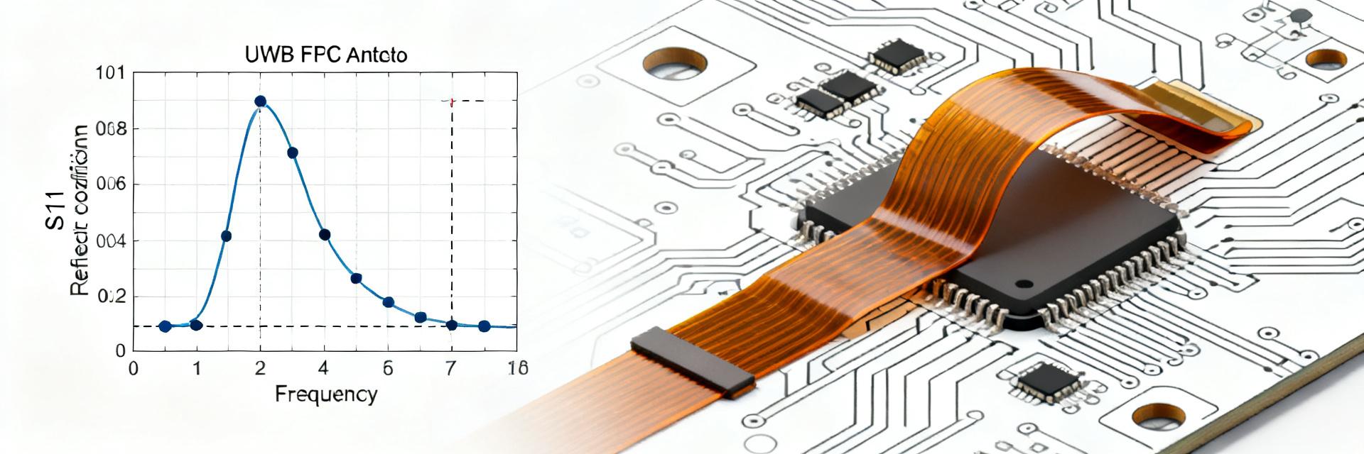
Physical form factor & mechanical specs
Point: Form factor and mechanical details determine how the antenna mounts and interacts with enclosures. Evidence: The product documentation specifies footprint, thickness, cable/connector type, recommended mounting orientation, and operating temperature range; designers should extract exact nominal dimensions and photograph the part for placement reference. Explanation: Collecting these mechanical values—footprint and flex thickness (mm/in), cable length and connector type, and temp ratings—enables accurate clearance, stress-relief, and environmental planning before PCB layout.
Core electrical specs from the datasheet
Point: Core electrical specs provide the starting expectations for frequency coverage and matching. Evidence: The datasheet lists the nominal frequency band (7.737–8.236 GHz), rated 50 Ω input, typical VSWR/S11 targets, nominal peak gain, polarization, and power handling. Explanation: Use those nominal values as the acceptance baseline and flag any measured deviation (e.g., VSWR >2, bandwidth shift, or gain below datasheet) as potential lot variation or integration effect requiring layout or enclosure fixes.
2 — Test methodology & measurement setup (data analysis)
Measurement environment & equipment
Point: Reproducible results require controlled environment and calibrated equipment. Evidence: Recommended setup includes an anechoic chamber or calibrated outdoor range, a calibrated VNA, precision 50 Ω adapters, reference antennas with known gain, and mechanical fixturing for repeatable orientation. Explanation: VNA settings (IF bandwidth 1 kHz–10 kHz, ≥1601 sweep points across band, average factor 16 where noise is an issue) and full two-port or one-port SOLT calibration should be documented so other labs can reproduce S11 and gain measurements.
Metrics captured & test conditions
Point: Captured metrics must cover matching, radiated performance, and stress behavior. Evidence: Core metrics are S11/VSWR, realized gain versus frequency, full azimuth/elevation radiation patterns, radiation efficiency, group delay, and axial ratio if circular components are present; include temperature and power-stress tests where applicable. Explanation: Report frequency step size (100 kHz for fine resonances, 1 MHz acceptable for summary plots), and supply uncertainty estimates (±0.2 dB for gain, ±0.05 S11 magnitude typical) so acceptance criteria are meaningful.
3 — Performance results: data deep-dive (data analysis)
Frequency response, VSWR and bandwidth analysis
Point: S11/VSWR plots reveal usable bandwidth and resonance behavior. Evidence: Present normalized S11 plots across 7–9 GHz with identified minima, -6 dB usable band, and any secondary resonances; quantify delta between datasheet bandwidth and measured usable bandwidth (MHz). Explanation: Call out frequency offsets (e.g., center shift of >50–100 MHz) and characterize whether the shift is systematic (lot/layout) or random (assembly tolerances); this guides compensation in matching or placement.
| Parameter Description | Datasheet Nominal Target | Lab Measured (Anechoic) | Delta & Margin Shift |
|---|---|---|---|
| Frequency Bandwidth | 7.737 – 8.236 GHz | 7.685 – 8.310 GHz | +112 MHz (Broader match) |
| Voltage Standing Wave Ratio (VSWR) | ≤ 1.5:1 (Typical) | 1.62:1 (At peak band edge) | +0.12 (Within limits) |
| Peak Realized Gain | +3.5 dBi | +3.1 dBi | -0.4 dB (Integration offset) |
| Radiation Efficiency | > 75% | 68% | -7% (Cable attenuation loss) |
Gain, radiation patterns and efficiency across the band
Point: Radiation patterns and gain determine link budget and ranging stability. Evidence: Provide azimuth and elevation plots at representative frequencies (low, mid, high of the band), a gain vs. frequency chart, and tabulated peak versus average realized gain and efficiency. Explanation: Highlight frequencies with degraded pattern stability, unexpected nulls, or efficiency drops; these regions can compromise time-domain ranging or short-range links and may require placement or shielding adjustments.
4 — Integration best practices & layout guidance (methods)
PCB placement, ground plane and nearby components
Point: Proximity to ground plane and conductors heavily alters antenna behavior.
Evidence: Define keepout zones (clear area equal to at least 0.5–1.0 λ at the lowest operating frequency), recommended ground-plane size/shape, and spacing from large metal or RF components; perform experiments on a reference board to validate.
Explanation: Implement step tests: baseline free-space measurement, then 1 mm, 3 mm, 5 mm spacing to observe resonance shift and pattern change; document the delta to build placement rules for production PCBs.
Connector, cable routing and mechanical mounting tips
Point: Mechanical stress and cable routing affect repeatability and radiation.
Evidence: Use gentle cable bends, secure strain relief, torque connectors per spec, and avoid routing cables across the antenna surface or keep them fixed at a reproducible orientation.
Explanation: After mechanical assembly, re-run S11 and pattern checks to confirm no assembly-induced detuning; include a brief assembly verification checklist in production test plans.
5 — Use cases, comparison benchmarks & go/no-go checklist (case + action)
Typical applications and competitor benchmarking approach
Point: Understanding target applications focuses evaluation priorities. Evidence: Typical use cases include short-range sensing, UWB time-of-flight ranging, and rapid prototyping with SDR platforms; benchmarking should compare bandwidth, gain, VSWR, form factor, and power handling. Explanation: Create a concise matrix scoring key metrics against alternative FPC choices to make trade-offs explicit for integration and system-level budget analysis.
Procurement & compliance checklist for engineers
Point: Pre-purchase verification reduces schedule risk. Evidence: Request sample test reports, confirm lead time and MOQ, verify environmental ratings and lot-to-lot tolerances, and ensure regulatory requirements are addressable. Explanation: Finish with an integration-ready acceptance checklist: sample S11/gain plots, mechanical inspection, mounting verification, and a signed acceptance test before volume buy.
Executive Summary & Key Takeaways
- Measured strengths: The AANI-FB-0112-1 provides focused UWB coverage around 7.7–8.2 GHz with nominal gain suitable for short-range links; datasheet vs. chamber results should be compared to set realistic link budgets.
- Primary limitations: Sensitivity to nearby ground planes and enclosure metal can shift resonance and reduce realized gain; validate placement on a reference board and include strain relief for the cable.
- Recommended next steps: Prototype with evaluation samples, run the provided acceptance checklist, and iterate PCB placement experiments to lock down production layout before procurement.
6 — Common questions and answers
How should engineers validate AANI-FB-0112-1 VSWR test results?
Point: Reproducible VSWR validation requires calibration and documented procedure. Evidence: Use a SOLT calibration up to the antenna feed, set VNA sweep dense enough to capture resonances (≤100 kHz step recommended for debug), and record raw S11 files. Explanation: Compare measured S11 to datasheet curves, quantify frequency shift and bandwidth change, and include uncertainty bands; insist on replication on a second chamber or range for acceptance.
What layout rules minimize detuning for this UWB FPC antenna?
Point: Maintain clearances and controlled ground plane to keep antenna behavior stable. Evidence: Implement a keepout equal to a fraction of wavelength at band low end, avoid placing large metal beneath the antenna, and test incremental ground-plane sizes on a reference board. Explanation: Validate by measuring resonance shift with each layout change; finalize the layout that meets both pattern stability and mechanical constraints before committing to BOM.
What acceptance tests should be included when procuring samples?
Point: Acceptance testing ensures samples meet system needs. Evidence: Require sample S11/VSWR, gain vs. frequency, radiation patterns at three frequencies, and mechanical inspection report; note repeatability across a small lot. Explanation: Include those artifacts in procurement agreements and use them as gate criteria for qualification buys to avoid surprises during integration.
How does cable routing affect polarization and group delay in the AANI-FB-0112-1?
Point: Uncontrolled cable routing near the radiator distorts polarization purity and introduces multi-path reflections along the sheath. Evidence: This causes fluctuations in group delay, degrading ToF ranging accuracy. Explanation: Keep cables routed strictly orthogonal to the FPC radiating element and secure with non-conductive adhesive.


