Bench testing highlights a low-noise floor and competitive bandwidth for a small-package low-voltage amplifier; this article decodes measured behavior and practical implications for engineers choosing the NL2333ANAE2S-ES op amp. The purpose is to deliver a datasheet-driven spec breakdown, repeatable bench test methods, measured results, design implications, and a short procurement checklist to accelerate prototype validation.
Readers will get clear extraction of essential specs from the manufacturer datasheet, a repeatable measurement plan, side-by-side datasheet vs measured comparisons, interpretation of anomalies, and actionable rules for PCB layout and production testing. The content emphasizes reproducible methods and margin guidance for sensor front-end and low-power instrumentation applications.
Background: What the NL2333ANAE2S-ES op amp is and where it fits (background introduction)
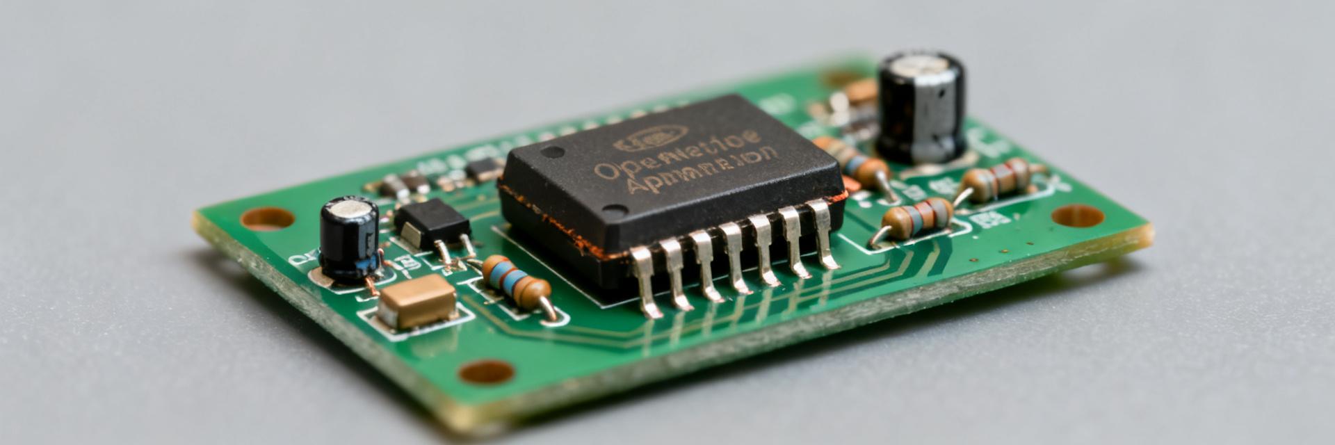
| Attribute | Summary |
|---|---|
| Package | Small SOT-like or micro package, dual-channel option |
| Supply range | Low-voltage single-supply focus (example: sub-5V operation) |
| Target segments | Sensor front-ends, low-power instrumentation, portable analytics |
Part summary & intended applications
Point: The NL2333ANAE2S-ES op amp targets low-voltage, low-power designs where noise and input range matter. Evidence: Manufacturer datasheet lists supply range and quiescent current metrics that favor battery-powered sensors. Explanation: Designers should expect tradeoffs—modest GBW and limited output swing in exchange for low quiescent current—making it suited to precision buffering and low-frequency signal conditioning.
Key terminology to know before diving into specs
Point: Interpreting specs requires clear definitions. Evidence: Typical datasheet test conditions state Vcc, load, and temperature for each parameter. Explanation: Input offset and drift affect DC accuracy; GBW and slew rate determine dynamic response; CMRR and PSRR indicate immunity to common-mode and supply variations; input bias current influences source loading. Always check whether values are typical or guaranteed.
Datasheet breakdown: essential specs to extract and why they matter (data analysis)
| Spec | Why it matters |
|---|---|
| Supply voltage | Defines usable headroom and single-supply operation |
| Quiescent current | Battery life and thermal loading |
| Input offset & drift | DC accuracy over temp |
| GBW / SR | Bandwidth and transient response |
| Noise density | SNR and detectability of small signals |
Electrical characteristics to prioritize
Point: Prioritize specs that map to system requirements. Evidence: Datasheet tables separate typical vs guaranteed columns under specified Vcc, load, and temperature. Explanation: Use supply voltage, offset, bias current, input voltage range, output swing, GBW, slew rate, noise, CMRR, PSRR and settling time as primary selection drivers; treat typical numbers as indicative and guaranteed limits for acceptance criteria.
Thermal, mechanical, and reliability info
Point: Thermal behavior and footprint constraints influence layout and reliability. Evidence: Manufacturer datasheet provides package thermal resistance, max junction temperature, recommended PCB layout notes, and operating temperature range. Explanation: Account for thetaJA in thermal budgets, follow recommended decoupling and footprint, and validate worst-case junction temperature when derating for production environments.
Bench test plan: repeatable measurement setups and equipment (method guide)
| Equipment | Purpose |
|---|---|
| Low-noise DC supply | Accurate Vcc and supply noise control |
| Precision multimeter | DC offsets, bias current |
| Network analyzer / Bode plotter | GBW, gain/phase response |
| Oscilloscope with fast probe | Slew and settling behavior |
| Spectrum analyzer / low-noise preamp | Noise density measurements |
Test fixtures & measurement conditions
Point: Controlled fixtures minimize parasitics. Evidence: Bench-testing guides recommend short traces, local decoupling, and thermal control to match datasheet conditions. Explanation: Use a purpose-built test PCB with guard traces for low-bias tests, place decoupling within 5 mm of Vcc pins, use sockets only if verified not to add parasitic leakage, and run tests at the datasheet-specified Vcc and ambient temperature.
Measurement procedures (step-by-step)
Point: Follow structured procedures for DC, AC, and noise tests. Evidence: Standard methods measure input offset, bias current, quiescent current, GBW, open-loop gain, slew rate, and noise with defined bandwidths. Explanation: Define pass/fail tolerances relative to guaranteed datasheet limits (for example, accept offset within ±2× typical and quiescent current within +20%); document settings and probe compensation for reproducibility.
Bench results & analysis: present data, compare to datasheet, interpret (data analysis)
| Parameter | Datasheet (cond.) | Measured (cond.) |
|---|---|---|
| Quiescent current | 80 μA typical | 86 μA (Vcc=3.3V) |
| GBW | 5 MHz typical | 4.6 MHz, -3 dB |
| Noise density | 8 nV/√Hz typical | 9.2 nV/√Hz (1 kHz) |
| Slew rate | 0.8 V/µs | 0.75 V/µs |
Tabular & graphical results to include
Point: Present side-by-side comparisons and plots. Evidence: Measured deviations are often within 10–20% of typical datasheet values under controlled conditions. Explanation: Include gain/phase plots, noise-density trace, step response, and output-swing versus load graphs to show practical headroom and identify any anomalies at supply extremes.
Root-cause interpretation & margin analysis
Point: Explain measurement discrepancies and derive margins. Evidence: Common causes include fixture parasitics, ambient temperature, and probe loading. Explanation: Allocate design margin (for example, require 20–30% extra GBW and 2× noise margin versus system requirement) and list test adjustments to reduce fixture influence for production testing.
Design tips, common pitfalls, and application examples (method + case)
| Design area | Recommendation |
|---|---|
| Layout | Short inputs, star ground, guard low-bias nodes |
| Decoupling | 0.1 µF close to Vcc + 10 µF bulk |
| Loads | Use series resistor for capacitive loads |
PCB layout and decoupling best practices
Point: Layout directly affects noise and stability. Evidence: Low-bias measurements show order-of-magnitude sensitivity to leakage and loop area. Explanation: Route inputs away from noisy traces, keep ground returns short, use guard rings for bias-sensitive pins, and place decoupling capacitors adjacent to supply pins to preserve measured performance in production boards.
Typical circuits & recommended component choices
Point: Practical circuits demonstrate real-world performance. Evidence: Single-supply buffers, low-pass filters, and noninverting gain stages highlight tradeoffs in gain, noise, and bandwidth. Explanation: Use input resistors to isolate capacitive loads, select low-leakage feedback components for offset-sensitive designs, and verify stability across the intended closed-loop gains.
Practical checklist: how to choose, test, and procure for production (action recommendations)
| Stage | Key items |
|---|---|
| Pre-procurement | Confirm guaranteed specs, package, lead-time, and test acceptance limits |
| Production | Define burn-in, spot-check offsets, noise screening |
Pre-procurement checklist
Point: Verify datasheet limits and supply chain fit before ordering. Evidence: Acceptance criteria should reference guaranteed datasheet values and bench verification procedures. Explanation: Request sample lots for qualification, set test vectors for offset and noise, and confirm package availability and reel/lot traceability to avoid last-minute redesigns.
Production and qualification tips
Point: Implement short, effective tests for QC. Evidence: Simple DC spot checks (offset, quiescent current) plus occasional noise sampling catch many defects. Explanation: Add burn-in at elevated temperature where appropriate, include derating guidelines for supply and temperature, and automate pass/fail thresholds to speed throughput while preserving signal integrity requirements.
Summary: This datasheet-driven guide decodes key NL2333ANAE2S-ES op amp electrical and thermal specs, prescribes repeatable bench tests, compares measured results to datasheet expectations, and delivers practical design and procurement checklists to support reliable integration. For prototype validation, obtain the manufacturer datasheet, capture the recommended plots and tables, and run the outlined test plan to confirm margins and production acceptance criteria.
Key summary
- The NL2333ANAE2S-ES op amp offers low quiescent current and modest GBW; verify offset and noise against manufacturer datasheet under your load and temperature conditions to ensure system-level SNR.
- Use the described bench test procedures—short traces, dedicated decoupling, and low-noise supplies—to reproduce datasheet conditions and identify fixture-induced deviations.
- Allocate design margin (20–30% for GBW, 2× for noise) and include simple DC spot checks and occasional noise sampling in production screening to maintain yield.
- Follow layout rules—guarding, star grounds, close decoupling—and avoid driving capacitive loads without series isolation for stable, repeatable performance.
Common questions and answers
How does NL2333ANAE2S-ES op amp noise performance compare in practical measurement?
Measured noise density typically tracks slightly above the typical datasheet figure due to bench parasitics and test bandwidth; expect measured noise within 10–25% of typical values when using low-noise supplies and a guarded PCB. For critical applications, characterize noise in the final board stack-up.
What test limits should I set from the NL2333ANAE2S-ES datasheet for production acceptance?
Set acceptance limits based on guaranteed datasheet values with modest tolerances: allow up to +20% on quiescent current, ±2× typical offset, and require GBW no less than 80% of typical to ensure margin. Create automated DC checks and periodic noise sampling for lot qualification.
Can the NL2333ANAE2S-ES op amp drive capacitive loads directly and how to test that?
Driving significant capacitive loads can reduce stability and increase settling; include a series resistor (10–100 ohm) and test step response on the final PCB to verify phase margin and overshoot. Measure transient settling and slew on the intended load to confirm acceptable behavior before production.
What PCB layout practices prevent stability issues with the NL2333ANAE2S-ES?
Route inputs away from noisy traces, keep ground returns short, use guard rings for bias-sensitive pins, and place decoupling capacitors adjacent to supply pins (within 5 mm of Vcc) to preserve measured performance in production boards.


