Bench and manufacturer figures show the AK323-2 delivering a compact power-management profile with standby currents in the single-digit microampere range and regulated outputs capable of supporting moderate loads — a key factor for designers targeting battery-powered instrumentation and portable control modules. This article walks through the AK323-2 datasheet with a clear, data-driven walkthrough of specs, pinout, thermal/mechanical limits, application guidance, and a verification checklist.
This guide emphasizes practical interpretation: how headline numbers translate to layout choices, safe operating margins, measurement steps, and example calculations that validate thermal and power behavior on the bench. Where useful, variants of the part and typical trade-offs are noted to help shorten prototype cycles while respecting device limits and reliability needs.
1 — Overview & Key Features (Background)
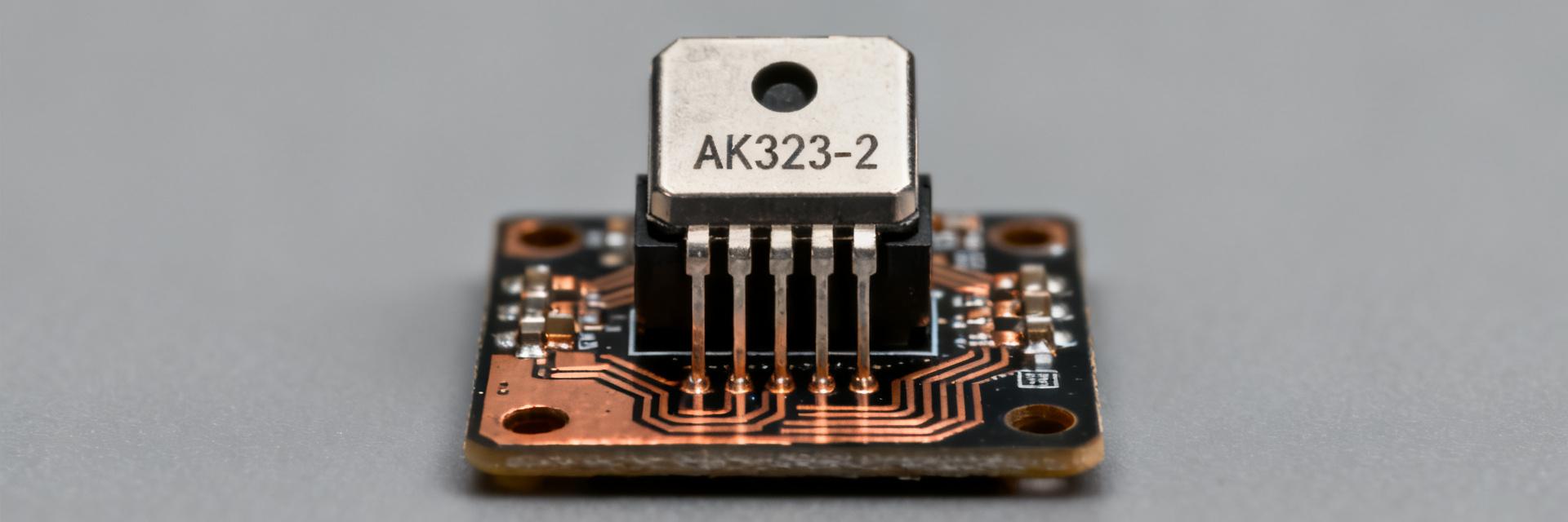
What the AK323-2 is
The AK323-2 is a compact analog regulator/mixed-signal IC intended for low-power embedded systems, sensor front-ends, and portable instrumentation. Engineers select it for a balance of low quiescent current, accurate regulation, and integrated monitoring or control pins. Practical highlights from the AK323-2 specs include tight output tolerance and features that reduce external component count for space-constrained PCBs.
At-a-glance spec summary
Use this compact spec snapshot for reference during schematic review and BOM freeze:
| Specification Parameter | Datasheet Value (Typical) | Conditions / Notes |
|---|---|---|
| Supply Voltage Range (V_IN) | 1.8V to 5.5V | Full operational envelope |
| Maximum Output Current (I_OUT) | 150 mA | Subject to thermal dissipation limits |
| Quiescent Standby Current (I_Q) | 1.2 µA | Low-power shutdown state, EN = Low |
| Output Regulation Accuracy | ±1.5% | Over full temperature and line limits |
| Thermal Junction-to-Ambient (θ_JA) | 120 °C/W | Standard 2-layer FR4 board layout |
2 — Pinout & Functional Block Diagram (Data analysis)
Pin definitions and recommended connections
- Power Pins (VIN, VOUT): Connect the input supply with low-ESR decoupling capacitors (0.1 µF ceramic + 1 µF to 10 µF tantalum/ceramic) as close to the device terminals as possible.
- Ground Pin (GND): Route directly to a single low-impedance star ground or system ground plane.
- Control Pins (EN, RST): Active high Enable (EN) and Reset (RST) pins require clean, bounce-free logic levels. If driven from noisy microcontrollers or long lines, add a local RC filter or pull-down resistor.
Functional block overview and signal flow
The internal architecture contains an ultra-stable bandgap reference, a linear regulator pass-transistor core, thermal protection circuitry, and a signal monitoring/comparator block. The general signal path routes from input to regulator and onward to the monitored outputs through internal voltage sense loops.
3 — Electrical Ratings & Performance (Data analysis)
Absolute maximum ratings vs. recommended operating conditions
Absolute maximum ratings define the physical boundaries beyond which permanent damage to the device may occur. Operating continuously at these limits degrades reliability. Maintain a safety margin: keep operating supply voltages 10% to 20% below the absolute maximum and restrict constant current loads to recommended levels.
Typical performance tables & real-world expectations
Quiescent current directly defines battery standby lifetimes, while thermal resistance determines safe load capabilities. Real-world dissipation calculations must prevent the junction temperature from exceeding maximum design limits.
4 — Thermal, Mechanical & Reliability Specs (Method/guide)
Thermal characteristics and PCB layout guidance
Implement the thermal resistance characteristics to design proper copper plane sizing and via placement:
- Layout Dos: Place thermal vias directly beneath the exposed ground paddle. Maximize available copper surface area on both outer layers of the PCB to act as heat spreaders. Keep input/output traces wide and short.
- Layout Don'ts: Do not route sensitive low-level analog or signal traces underneath or adjacent to hot thermal pathways. Avoid bottlenecking the return ground current loop.
Package, footprint, and environmental ratings
Ensure that footprints match standard manufacturer IPC-7351 guidelines. Confirm the operating temperature profile, storage humidity limits, and moisture sensitivity levels (MSL) conform to the physical assembly line profile. Selecting matched materials avoids stress fractures and early board wear out in high-vibration applications.
5 — Application Examples & Design Guidelines (Case display / Method)
Typical application circuits
- Example A: Regulated Power Stage for Low-Noise Sensors
Configures the regulator with a 10 µF low-ESR ceramic capacitor on the output and a local 0.1 µF bypass capacitor immediately at the supply pins to maximize transient suppression. - Example B: Monitored Supply Rail with Comparator Flag
Integrates an external RC delay filter on the Reset (RST) output to eliminate transient switching noise, keeping comparator threshold accuracy clean.
Measurement & verification checklist for prototypes
- [ ] Measure and verify quiescent current draw (I_Q) matches datasheet curves within ±20% under zero-load conditions.
- [ ] Confirm output voltage regulation remains within tolerance throughout the input sweep range.
- [ ] Record local package temperature rise during steady-state, maximum load operations.
- [ ] Verify operational logic threshold values for Enable and Reset startup timings on an oscilloscope.
6 — Testing, Compliance & Troubleshooting (Action suggestions)
Recommended tests and compliance considerations
Run formal verification tests, including IV characteristic curves, step-load transient responses, thermal stress cycling, and near-field electromagnetic compatibility (EMC) pre-compliance scanning. If marginal EMC issues are detected near critical operating frequencies, introduce a series ferrite bead or common-mode filter to smooth out high-frequency switching lines.
Common failure modes and fixes
- Symptom: Excessive heat or thermal shutdown.
Fix: Increase copper pad area or introduce additional ground-plane thermal stitching vias near the IC. - Symptom: Output oscillations or ripple.
Fix: Place low-ESR ceramic decoupling capacitors physically closer to the device pins to minimize parasitic inductance. - Symptom: Spurious resets or startup glitches.
Fix: Add an RC filter delay on the Enable (EN) input to damp transient startup noise spikes.
Summary
- The AK323-2 datasheet highlights a low-quiescent, moderate-current regulator with clear operating vs absolute limits; designers should prioritize decoupling and thermal copper to meet AK323-2 specs in compact builds.
- Key design warnings: stay below absolute maximums with a 10–20% safety margin, follow recommended footprint and via layout to control junction rise, and validate comparator or control pins with bench threshold tests tied to AK323-2 ratings.
- Run the verification checklist early: measure quiescent/current draw, validate regulation under load, and perform a thermal soak to confirm PCB-level dissipation matches calculations before assembly sign-off.
Frequently Asked Questions
How do AK323-2 specs affect battery life estimates?
Estimate battery life by combining quiescent current and active duty-cycle current from the AK323-2 specs with system load. Calculate average current (Iq + active_load × duty_cycle) and divide battery capacity (mAh) by average current to get hours. Include margin for self-discharge and peripheral consumption to avoid optimistic runtime claims.
What steps should I follow to validate AK323-2 thermal behavior on a prototype?
Measure power dissipation under worst-case load, then apply the datasheet junction-to-ambient thermal resistance to predict temperature rise. Place a thermocouple on the package, run a steady-state load until temperatures stabilize, and compare measured rise to the calculated value. If high, increase copper area or add thermal vias.
Which tests confirm AK323-2 ratings during production screening?
Production screening should include a power-up functional test, output-voltage tolerance check under nominal and maximum load, a brief thermal stress at elevated ambient, and a control-pin functional check. Failures clustering on thermal or stability tests usually indicate layout or soldering issues rather than device intrinsic faults.
What is the recommended decoupling capacitance for AK323-2 stability?
For standard operations, place a high-quality 0.1 µF ceramic capacitor in parallel with a 1.0 µF to 10 µF low-ESR capacitor directly across the input and output pins. Ensure these capacitors are located within 2mm of the IC physical footprint to minimize parasitic trace inductance.


