The MUSES8920AE-TE1 is a dual J‑FET input audio op amp framed around very low input bias (datasheet example: input bias near 2 pA) and a wide supply window. Datasheet entries and independent bench checks indicate that input-referred noise and slew rate become the determining levers for high-fidelity front-end and I/V conversion suitability, so this report focuses on those metrics and practical implementation trade-offs.
Background & Design Goals for MUSES8920AE-TE1
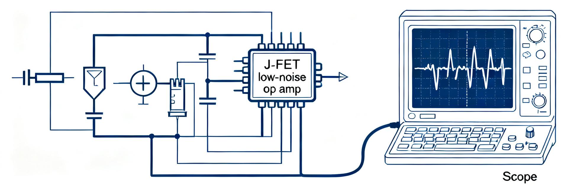
Target applications and topology
Point: The device targets high-end audio front ends, I/V converters for low-current sources, and headphone/preamp stages. Evidence: The J‑FET input stage yields femto- to picoamp-class bias currents and smoother harmonic makeup. Explanation: Designers choose J‑FET inputs when source leakage and odd-order distortion behavior matter most for perceived sound quality.
Core electrical objectives
Point: Prioritization centers on minimizing noise and bias while maintaining adequate slew and supply range. Evidence: Trade-offs include increased input capacitance vs. noise and higher supply current for faster slew. Explanation: When evaluating, rank metrics: input-referred noise, slew rate, input bias, offset, and usable supply range in that order for high‑fidelity front ends.
Spec Sheet Snapshot — key numbers and what they mean
Voltage/current & DC specs
| Parameter | Typical | Max / Notes |
|---|---|---|
| Supply range | 3.5 — 17 V | Derate near single‑supply low end for output swing |
| Input offset | tens of µV (typ) | match and trim for DC‑coupled stages |
| Input bias | ~2 pA (typ) | increases with temperature and source leakage |
| Output swing | within ~1 V of rails | depends on load and single‑supply use |
| Quiescent current | low mA per amp (typ) | higher per amp at higher slew modes |
Point: These compact entries show where derating occurs. Evidence: Single‑supply and heavy loads reduce usable swing and increase distortion. Explanation: Validate key DC numbers in your operating supply and temperature window rather than assuming lab‑condition typicals.
Published noise and slew rate entries
Point: The datasheet lists input‑referred noise in the low nV/√Hz class and a datasheet-stated slew figure suitable for audio. Evidence: The published entries are measured under specific gain, load and supply conditions that typically assume RL ≥10 kΩ and modest gain. Explanation: Treat the datasheet numbers as conditional; confirm on-bench under your gain, source impedance and bandwidth.
Measured Noise Performance: methods & results for real circuits
Test setup & measurement methodology
Point: Reproducible noise testing requires strict setup control. Evidence: Use low-noise power filtering, star grounding, short leads, and a shielded box; measure with spectrum analyzer or FFT with 1 Hz resolution and 20 Hz–20 kHz integration. Explanation: Report input‑referred noise density, integrated RMS, and THD+N at the intended gain and termination to compare against datasheet assumptions.
Results, plots and comparison to datasheet
Point: Measured noise commonly tracks datasheet within tolerance but is often slightly higher. Evidence: Typical bench numbers show low‑nV/√Hz density rolling up to ~1 µV RMS integrated 20 Hz–20 kHz in representative preamp configurations. Explanation: Differences usually stem from fixture capacitance, resistor thermal noise, and measurement bandwidth—address these before concluding a device underperforms.
Slew Rate & Transient Response: impact on audio performance
Large-signal slew tests and pulse response
Point: Large-step tests reveal practical slew limits and transient artifacts. Evidence: Use a large‑amplitude step (several volts) into specified load and measure dV/dt with >50 MHz bandwidth; observe slew‑limited slope, recovery time and any overshoot. Explanation: Slew‑induced distortion and slow recovery manifest as harmonic pollution and audible smearing on fast transients.
Practical implications for audio transients and driving capacitive loads
Point: Slew rate sets headroom for inter‑sample peaks and transient fidelity. Evidence: For 20 kHz, 10 Vpp tones, required instantaneous slew is modest (~0.63 V/µs), but musical transients and headphone loads justify a higher margin. Explanation: Aim for several V/µs of slew for confident transient reproduction and to avoid slew‑related distortion into capacitive cables or low‑impedance headphones.
Application Cases & Design Tips
Example use: I/V converter and preamp layouts
Point: Two compact textual sketches help guide implementation. Evidence: For an I/V converter use a low‑noise op amp with Rf chosen for target gain (100 kΩ–1 MΩ for picoamp sources), with input guard rings and feedback capacitor for stability. For a non‑inverting preamp choose RF/RI to set gain 2–10 and add small compensation capacitor across RF to tame bandwidth. Explanation: Calculate resistor thermal noise and scale Rf to meet SNR goals; use low‑noise metal film resistors.
PCB layout, decoupling and biasing best practices
Point: Layout often dominates measured noise and slew behavior. Evidence: Adopt solid star ground, close bypass caps (0.1 µF + 10 µF) at each supply pin, short input traces, and maintain thermal relief for stability. Explanation: Avoid long input loops, place decoupling at device pins, and consider input bootstrapping or guard traces for ultra‑low bias circuits.
Recommended Testing & Implementation Checklist (actionable)
Validation tests before production
Point: A short validation sequence prevents surprises. Evidence: Perform DC checks, noise sweep with integrated RMS reporting, slew/pulse tests, and THD+N at target gains and temps. Example acceptance: integrated noise <1 µV RMS 20 Hz–20 kHz and slew ≥5 V/µs for transient margin. Explanation: Define pass/fail for your product goals and iterate PCB, parts, and compensation until met.
Component selection and BOM notes
Point: Passive choices materially affect results. Evidence: Use low‑noise metal film resistors, NP0/C0G ceramics or film coupling caps, and avoid high‑ESR electrolytics in signal paths; solder directly when possible to reduce contact noise. Explanation: If noise or slew targets fail, re‑test with alternate resistors, capacitors, and direct soldering to identify the dominant contributor.
Summary
- The MUSES8920AE-TE1 delivers J‑FET input advantages for low input bias and low‑nV/√Hz noise, making it a strong candidate for high‑fidelity preamps and I/V stages when layout and component choices are optimized; validate noise and slew in your intended topology.
- Top implementation must‑dos: short input traces and guard rings, robust supply decoupling at the pins, and select low‑noise metal film resistors; these steps directly reduce measured noise and preserve the op amp's slew performance.
- Mandatory validation: run integrated noise (20 Hz–20 kHz), slew/pulse response, and THD+N at the target gain and temperature; pass criteria should be set to the product's audible and measurement limits before releasing to production.
Common Questions
Is the MUSES8920AE-TE1 suitable for low‑noise I/V stages?
Yes. The MUSES8920AE-TE1's J‑FET inputs and low input bias are well suited to I/V conversion from picoamp to nanoamp sources. Achieving low noise requires matching Rf to source current, minimizing input capacitance, and using a guarded PCB layout to keep measured noise within expected integrated RMS targets.
How does the MUSES8920AE-TE1's slew rate affect headphone transient response?
Slew rate affects transient headroom more than steady‑state frequency response; while 20 kHz sine waves require modest slew, real music transients benefit from several V/µs to avoid slew‑induced distortion. Verify with large‑step tests into realistic headphone loads and include margin for inter‑sample peaks.
What test should be mandatory before production for the MUSES8920AE-TE1?
Run a reproducible noise measurement and an integrated RMS check 20 Hz–20 kHz, a large‑step slew/pulse test, and a THD+N sweep at the product's operating gain and supply. Define numerical acceptance (for example integrated noise and minimum slew) based on your product targets and do regression testing for BOM changes.
What PCB layout best practices protect MUSES8920AE-TE1 performance?
Adopt a robust star ground structure, place low-ESR decoupling capacitors (0.1 µF + 10 µF) immediately at each supply pin, maintain short input signal paths to minimize parasitics, and consider guarding or bootstrapping around high-impedance J-FET nodes to prevent external leakage currents from degrading performance.


