Engineers typically scan a component datasheet for a short list of mission-critical numbers before approving a part for design. This article converts the raw datasheet into actionable guidance by focusing on the electrical and thermal figures that determine system fit, and by giving repeatable checks to verify that the device meets project requirements.
The presentation emphasizes practical extraction: part decoding, absolute maximums, operating ranges, thermal derating, reliability signals, verification calculations, and PCB/layout actions engineers use to move from datasheet to prototype-ready selection.
Background & part identification
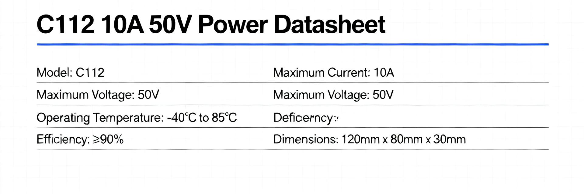
Part-number decoding and variant notes
Point: The part code segments encode package, current/voltage class, and revision. Evidence: C112 10A043 050 10 typically implies a 10 A current class and a 50 V voltage class, with middle fields denoting internal revision and tolerance. Explanation: Flag ambiguous fields on vendor documents and always confirm the mechanical drawing and marking to avoid version mismatches.
Typical applications and system-level fit
Point: The device is suited to power switching, protection, and motor-drive front ends. Evidence: The combination of multi-ampere continuous current and moderate voltage rating maps to DC-DC outputs and load switches. Explanation: Match space, expected lifetime, thermal budget, and transient behavior to system-level parameters when evaluating suitability.
Full specifications & electrical ratings (core specs & ratings)
Absolute maximum ratings — what to extract and present
Point: Extract absolute maximums early to set safety limits. Evidence: Key limits include maximum voltage, continuous and peak current, power dissipation, and junction temperature range. Explanation: Present these as a clear table and highlight derating boundaries so design rules enforce safe operation under worst-case ambient conditions.
| Parameter | Symbol | Value (typ/max) | Units | Notes |
|---|---|---|---|---|
| Maximum DC voltage | Vmax | 50 | V | Absolute clamp; do not exceed |
| Continuous current | Icont | 10 | A | At specified Ta and PCB mounting |
| Peak pulse current | Ipk | 20 (10 ms) | A | Short-duration rating |
| Power dissipation | Pd | 3 | W | Max at Ta with recommended heatsink |
| Junction temperature | Tj | -55 to 150 | °C | Operating limits |
Recommended operating conditions & electrical characteristics
Point: Capture nominal operating ranges and test conditions. Evidence: Important entries include nominal voltage/current, on-resistance or conduction drop, leakage, switching times, and capacitances with their test setups. Explanation: Note the temperature and circuit used for each spec; real-world performance shifts with higher ambient and circuit parasitics.
Performance data & validation (data analysis)
Thermal performance and derating curves
Point: Thermal resistance and derating curves determine allowable continuous power by ambient. Evidence: Extract thetaJA/thetaJC and the ambient-derating graph. Explanation: Convert curves into PCB thermal requirements: required copper area, thermal vias, and external heatsinking to keep junction below specified max under worst-case load.
Reliability, lifetime & test results
Point: Reliability metrics guide end-of-life expectations. Evidence: Look for HTOL, cycling, and any MTTF/MTBF figures or qualification logs. Explanation: If the datasheet omits endurance data, plan accelerated stress tests and include margin in warranty calculations; treat unspecified lifetime as a signal to validate in-house.
How to read and verify the C112 10A043 050 10 datasheet
Cross-checking specs with system requirements
Point: Use a checklist to confirm compatibility. Evidence: Verify each spec against system worst-case values for voltage, current, and temperature and apply safety factors. Explanation: Recommended margins: +20% for continuous current, +30% for voltage transients unless protected, and derate for high ambient; document any mismatches before prototyping.
Simple verification calculations and example use-cases
Point: Run quick junction-temperature and derating math. Evidence: Compute Tj = Ta + (Pd × thetaJA) using expected Pd under load. Explanation: Example — at 2 W dissipation and thetaJA 40 °C/W, Tj rises 80 °C above ambient; if ambient is 50 °C, junction reaches 130 °C, requiring additional cooling or lower load.
Practical selection, PCB layout & application tips
Choosing safety margins, fusing and protection
Point: Select margins and protection based on datasheet pulse ratings. Evidence: Use pulse current data for inrush and short events and the continuous rating for steady-state. Explanation: Fuse current should be sized to allow safe steady energy but blow under sustained overcurrent; consider TVS or snubbers for voltage transients.
PCB layout, thermal vias, and assembly considerations
Point: Layout drives thermal performance. Evidence: Datasheet pad recommendations and thermal via guidance indicate required copper area and via count. Explanation: Use a copper pour tied to the device pad, place a dense via array under the thermal pad, and follow solder paste recommendations to ensure consistent thermal contact and reliable solder joints.
Summary
- Decode the part number to confirm package, current, and voltage class; confirm ambiguous fields against mechanical drawings before purchase.
- Extract absolute maximums and operating specs into a single table of specs and ratings so system limits are explicit and enforceable during design reviews.
- Convert thermal numbers (thetaJA/thetaJC and derating curves) into PCB copper, via, and heatsink requirements and run junction-temperature checks before prototype.
- Verify reliability signals and run targeted validation tests—steady-state current, thermal imaging, and HTOL-style stress—prior to production sign-off.


