Introduction: The MUSES8920 family is specified with ultra-low noise (≈8.0 nV/√Hz) and extremely low distortion (≈0.0004% THD+N at 1 kHz), figures that directly affect perceived clarity in high-end preamps and portable audio designs. This deep dive parses the MUSES8920AKX7-TE3 variant, translating datasheet numbers into practical design decisions and repeatable lab procedures a US-based engineer can run with common bench gear.
The authoritative MUSES8920 datasheet is the baseline for guaranteed and typical numbers; this article treats those figures as starting points and focuses on how to reproduce, interpret, and tune for them in a real PCB and test environment.
1 — Background: What MUSES8920AKX7-TE3 Is and Where It Fits
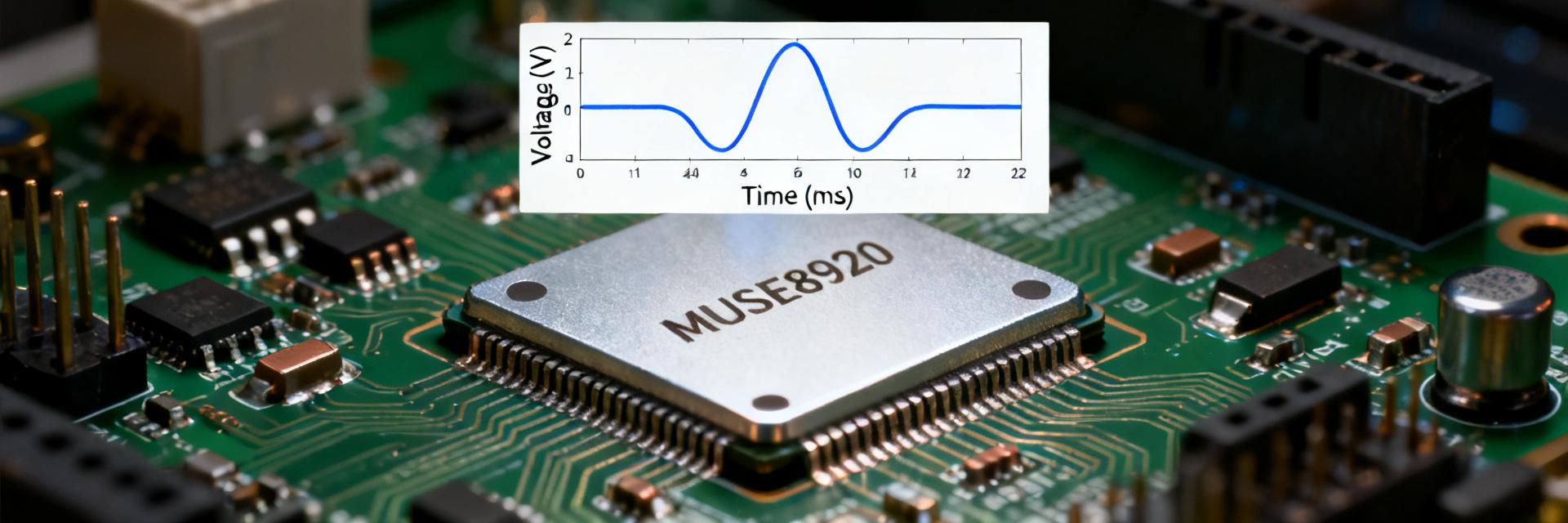
Device overview & package/pin summary
Point: The MUSES8920AKX7-TE3 is an audio op-amp family member targeted at high-end and portable audio where noise and distortion dominate subjective quality. Evidence: datasheet tables show low noise density and low THD+N at small-signal conditions. Explanation: Designers should view this part as a precision audio amplifier optimized for low-level stages in preamps and headphone buffers. Compatibility checklist: verify supply rails (single vs dual allowed), rail‑to‑rail expectations (not full RR outputs), and recommended load limits before integration.
Key specs at a glance
| Specification Parameter | Typical Value | Design Significance |
|---|---|---|
| Noise Density | ~8.0 nV/√Hz | Minimizes input-referred noise floor in high-gain stages. |
| THD+N | ≈0.0004% (@ 1 kHz) | Ensures absolute waveform fidelity and transparent rendering. |
| Slew Rate | Moderate (Typical) | Sufficient for full power output within the audio bandwidth. |
| Input Impedance | High (Low Bias Current) | Ideal for high-impedance volume controls and filter networks. |
| Output Swing | Load Dependent | Limited by supply rails; requires headroom margin tracking. |
2 — Data Analysis: Interpreting Electrical Performance
Noise & distortion decoded
Point: Noise density in nV/√Hz must be integrated across the audible band to get RMS noise. Evidence: using 8.0 nV/√Hz and bandwidth 20 Hz–20 kHz, RMS noise ≈ 8e‑9 × √(19,980) ≈ 1.13 µV RMS. Explanation: that equates to roughly −119 dBV; for a 2 Vrms full-scale output the SNR is ≈125 dB, showing why ultra-low noise matters in preamp front ends. THD/THD+N must be interpreted with the test gain, output level, and load; replicate those conditions when comparing to the datasheet to avoid misleading conclusions. Use consistent filters (IEC/AES or 20 Hz–20 kHz) and averaging to avoid measurement bias.
Frequency response, slew rate and dynamic behavior
Point: Bandwidth and slew rate determine transient fidelity and maximum undistorted slew for large steps. Evidence: datasheet bandwidth and slew-rate entries set practical thresholds (e.g., minimum slew per gain to reproduce a given square-wave amplitude). Explanation: for example, required slew ≈ 2π·f·Vpk — if the part’s slew is lower than that threshold distortion appears on fast transients. PSRR and CMRR numbers indicate how sensitive the amplifier is to supply and common‑mode noise; in practice, robust decoupling reduces measured PSRR degradation in a real front-end.
3 — How to Test MUSES8920AKX7-TE3: Lab Setups & Procedures
Bench setup for noise, THD+N and frequency response
Point: Reproducible measurements need a defined chain: low-noise power supply, precision signal source, audio analyzer, shielding, and the DUT on a minimal test PCB. Evidence: match the datasheet test conditions—gain, output amplitude, load, and filter settings (use the same weighting/AES filters). Explanation: recommended parameters: gain = +6 dB (or datasheet gain), input amplitude to yield the specified output, load = datasheet value (e.g., 2 kΩ), bandwidth = 20 Hz–20 kHz (or AES17), averaging off for THD but enabled for noise floor checks. Calibrate out analyzer noise by shorting inputs and subtracting system contribution where supported.
Power, thermal and stability testing
Point: Measure quiescent current, thermal rise, and oscillation margin under intended loads. Evidence: monitor supply current with a low‑ohm series resistor and use thermal imaging at typical ambient. Explanation: run long‑duration power‑on tests at worst-case supply and load, check junction/board temperature rise, and test stability with increased capacitive load and series isolating resistor values; add series resistance or compensation networks if oscillation is seen.
4 — Case Study: Building a Headphone Preamp with MUSES8920AKX7-TE3
Test-build overview and expected metrics
Point: A single-stage preamp using this part should target low gain and low output impedance for headphones. Evidence: with correct feedback resistor values and output coupling, expected noise floor matches integrated datasheet noise and undistorted output into 32–300 Ω loads approaches specified swing. Explanation: use input resistors in 10 kΩ–100 kΩ range, set feedback to realize the desired gain while keeping input-referred noise low; choose supply rails that provide required headroom for desired output into common headphone impedances.
Measured vs datasheet: troubleshooting and tuning
Point: Layout, grounding, and decoupling explain most discrepancies between bench and datasheet. Evidence: common issues include high loop area, long input traces, and inadequate bypassing that raise measured noise or THD. Explanation: isolate noise by shielding inputs, use local decoupling (0.1 µF + 10 µF) close to pins, shorten feedback traces, and re-run measurements after each change following the prioritized checklist below to close the gap to datasheet numbers.
5 — Actionable Design & Selection Checklist
When to choose MUSES8920AKX7-TE3
- Choose when ultra-low noise and ultra-low THD+N are top priorities (audiophile preamps, critical mic front-ends).
- Avoid if cost, extreme rail-to-rail swing, or high output drive into very low impedances are primary constraints—consider fuller‑featured buffers then.
- Match supply margins and expected load to the device’s recommended ranges before final selection.
PCB layout, decoupling and final validation checklist
- Decoupling: 0.1 µF ceramic close to each supply pin plus 10 µF bulk; place return vias adjacent to pins.
- Grounding: Star or split analog ground with single point tie to chassis; minimize loop areas for inputs/feedback.
- Validation tests: Noise (20 Hz–20 kHz), THD+N at specified gain and load, PSRR, CMRR, stability with capacitive loads; pass/fail thresholds tied to datasheet specs.
Summary
- The MUSES8920AKX7-TE3 delivers class-leading noise and distortion metrics suitable for high-end audio stages when integrated with careful layout and supply practices; consult the MUSES8920 datasheet for baseline guaranteed values.
- Datasheet numbers are reproducible with disciplined measurement: match gain, load, filter, and averaging settings; calibrate system noise out of results.
- Use the provided test recipes, decoupling and layout checklist to validate parts in your system and minimize mismatch between datasheet and measured results.
Frequently Asked Questions
How does MUSES8920AKX7-TE3 noise performance translate to SNR in a preamp?
With a noise density near 8.0 nV/√Hz, integrate across 20 Hz–20 kHz to get ≈1.1 µV RMS. For a 2 Vrms full-scale output that produces an SNR near 125 dB. Real systems will show lower SNR if PCB noise, power supply noise, or gain-stage choices increase the input‑referred noise.
What test procedure yields a valid THD+N figure for MUSES8920AKX7-TE3?
Use a precision audio analyzer, set gain to the datasheet condition, drive the input to produce the specified output, load per datasheet, and use a 20 Hz–20 kHz or AES17 filter. Turn off averaging for distortion, ensure system calibration, and subtract analyzer noise when possible to match datasheet methodology.
What are the common layout fixes when measured distortion exceeds the MUSES8920AKX7-TE3 datasheet?
Prioritize short feedback and input traces, local decoupling (0.1 µF + 10 µF), solid star grounding, and input shielding. If instability appears with capacitive loads, add small series output resistance (10–100 Ω) or compensation networks and re-check THD+N after each change.
What are the optimal power supply decoupling guidelines for the MUSES8920AKX7-TE3?
Place a 0.1 µF ceramic capacitor in parallel with a 10 µF bulk electrolytic capacitor close to each supply pin. Return vias must be placed immediately adjacent to the ground pins to minimize inductive loop areas and block high-frequency supply line noise.


